www.ti.com
SN74HC02, SN54HC02 SCLS076G – DECEMBER 1982 S– NRE7V4IHSECD0D2E,CSENM5B4EHR C200220
SCLS076G – DECEMBER 1982...
www.ti.com
SN74HC02, SN54HC02 SCLS076G – DECEMBER 1982 S– NRE7V4IHSECD0D2E,CSENM5B4EHR C200220
SCLS076G – DECEMBER 1982 – REVISED DECEMBER 2020
SNx4HC02 Quadruple 2-Input Positive-NOR Gates
1 Features
Buffered inputs Wide operating
voltage range: 2 V to 6 V Wide operating temperature range:
–40°C to +85°C Supports fanout up to 10 LSTTL loads Significant power reduction compared to LSTTL
logic ICs
2 Applications
Alarm / tamper detect circuit S-R latch
3 Description
This device contains four independent 2-input NOR gates. Each gate performs the Boolean function Y = A + B in positive logic.
Device Information
PART NUMBER
PACKAGE(1)
BODY SIZE (NOM)
SN74HC02D
SOIC (14)
8.65 mm × 3.90 mm
SN74HC02DB
SSOP (14)
6.20 mm × 5.30 mm
SN74HC02N
PDIP (14)
19.30 mm × 6.40 mm
SN74HC02NS
SO (14)
10.20 mm × 5.30 mm
SN74HC02PW
TSSOP (14)
5.00 mm × 4.40 mm
SN54HC02J
CDIP (14)
19.94 mm × 7.62 mm
SN54HC02W
CDIP (14)
9.20 mm × 6.29 mm
SN54HC02FK
LCCC (20)
8.89 mm × 8.89 mm
(1) For all available packages, see the orderable addendum at the end of the data sheet.
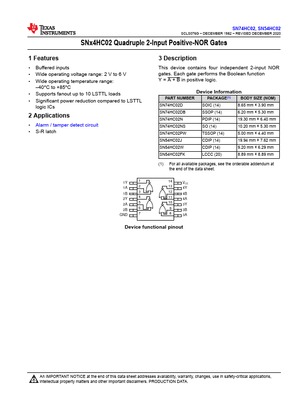
1Y
1
1A
2
1B
3
2Y
4
2A
5
2B
6
GND
7
14
VCC
13
4Y
12
4B
11
4A
10
3Y
9
3B
8
3A
Device functional pinout
CopyrighAtn©I2M0P20OTReTxaAsNInTsNtruOmTeInCtsEInactotrhpeoreatnedd of this data sheet addresses availability, warranty, changes, use iSnusbamfeittyD-corcituicmael anpt pFleiceadtbioancsk,
1
intellectual property matters and other important disclaimers. PRODUCTION DAT...