SN74HC10ĆEP TRIPLE 3ĆINPUT POSITIVEĆNAND GATE
D Controlled Baseline
− One Assembly/Test Site, One Fabrication Site
D Ex...
SN74HC10ĆEP TRIPLE 3ĆINPUT POSITIVEĆNAND GATE
D Controlled Baseline
− One Assembly/Test Site, One Fabrication Site
D Extended Temperature Performance of
−40°C to 125°C
D Enhanced Diminishing Manufacturing
Sources (DMS) Support
D Enhanced Product-Change Notification D Qualification Pedigree† D Wide Operating
Voltage Range of 2 V to 6 V
† Component qualification in accordance with JEDEC and industry standards to ensure reliable operation over an extended temperature range. This includes, but is not limited to, Highly Accelerated Stress Test (HAST) or biased 85/85, temperature cycle, autoclave or unbiased HAST, electromigration, bond intermetallic life, and mold compound life. Such qualification testing should not be viewed as justifying use of this component beyond specified performance and environmental limits.
SCLS558 − JANUARY 2004
D Outputs Can Drive Up To 10 LSTTL Loads D Low Power Consumption, 20-µA Max ICC D Typical tpd = 9 ns D ±4-mA Output Drive at 5 V D Low Input Current of 1 µA Max
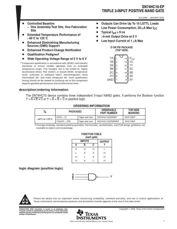
D OR PW PACKAGE (TOP VIEW)
1A 1 1B 2 2A 3 2B 4 2C 5 2Y 6 GND 7
14 VCC 13 1C 12 1Y 11 3C 10 3B 9 3A 8 3Y
description/ordering information
The SN74HC10 device contains three independent 3-input NAND gates. It performs the Boolean function Y = A B C or Y = A + B + C in positive logic.
ORDERING INFORMATION
TA
PACKAGE‡
ORDERABLE PART NUMBER
TOP-SIDE MARKING
SOIC − D −40°C to 125°C
TSSOP − PW
Tape and reel Tape and reel
SN74HC10QDREP SN74HC10QPWREP
SHC10EP SHC10EP
‡ Package dr...