SN74HC166AĆQ1 8ĆBIT PARALLELĆLOAD SHIFT REGISTER
SCLS538A − AUGUST 2003 − REVISED APRIL 2008
D Qualified for Automotiv...
SN74HC166AĆQ1 8ĆBIT PARALLELĆLOAD SHIFT REGISTER
SCLS538A − AUGUST 2003 − REVISED APRIL 2008
D Qualified for Automotive Applications
D Low Input Current of 1 µA Max
D ESD Protection Exceeds 2000 V Per
D Synchronous Load
MIL-STD-883, Method 3015; Exceeds 200 V Using Machine Model (C = 200 pF, R = 0)
D Wide Operating
Voltage Range of 2 V to 6 V
D Direct Overriding Clear D Parallel-to-Serial Conversion
D Outputs Can Drive Up To 10 LSTTL Loads
D Low Power Consumption, 80-µA Max ICC D Typical tpd = 13 ns D ±4-mA Output Drive at 5 V
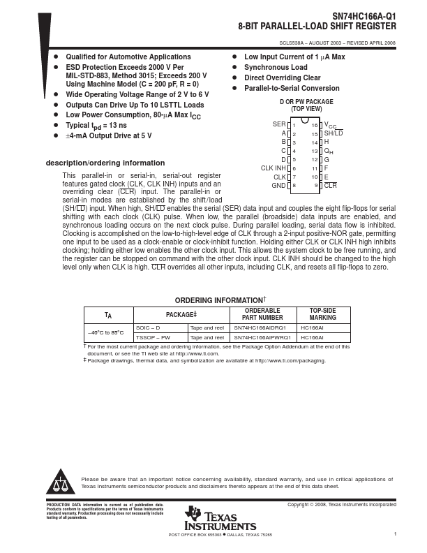
D OR PW PACKAGE (TOP VIEW)
SER A B
1 2 3
16 VCC 15 SH/LD
14 H
description/ordering information
This parallel-in or serial-in, serial-out register features gated clock (CLK, CLK INH) inputs and an overriding clear (CLR) input. The parallel-in or
C D CLK INH CLK GND
4 5 6 7 8
13 QH 12 G 11 F 10 E 9 CLR
serial-in modes are established by the shift / load
(SH/LD) input. When high, SH/LD enables the serial (SER) data input and couples the eight flip-flops for serial
shifting with each clock (CLK) pulse. When low, the parallel (broadside) data inputs are enabled, and
synchronous loading occurs on the next clock pulse. During parallel loading, serial data flow is inhibited.
Clocking is accomplished on the low-to-high-level edge of CLK through a 2-input positive-NOR gate, permitting
one input to be used as a clock-enable or clock-inhibit function. Holding either CLK or CLK INH high inhibits
clocking; holding either low enables the other c...