SN54HC175, SN74HC175
SCLS299F – JANUARY 1996 – REVISED JUNE 2022
SNx4HC175 Quadruple D-Type Flip-Flops With Clear
1 Fea...
SN54HC175, SN74HC175
SCLS299F – JANUARY 1996 – REVISED JUNE 2022
SNx4HC175 Quadruple D-Type Flip-Flops With Clear
1 Features
Wide operating
voltage range of 2 V to 6 V Outputs can drive up to 10 LSTTL Loads Low power consumption, 80-μA max ICC Contain four flip-flops with double-rail outputs Typical tpd = 13 ns ±4-mA output drive at 5 V Low input current of 1 μA max
2 Applications
Buffer/storage registers Shift registers Pattern generators
3 Description
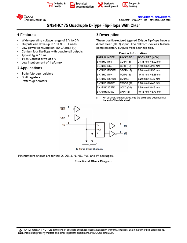
These positive-edge-triggered D-type flip-flops have a direct clear (CLR) input. The ’HC175 devices feature complementary outputs from each flip-flop.
PART NUMBER SN54HC175J SN74HC175D SN74HC175DBR SN74HC175N SN74HC175NSR SN74HC175PW SNJ54HC175FK SNJ54HC175W
Device Information
PACKAGE(1) BODY SIZE (NOM)
CDIP (16)
24.38 mm × 6.92 mm
SOIC (16)
9.90 mm × 3.90 mm
SSOP (16)
6.20 mm × 5.30 mm
PDIP (16)
19.31 mm × 6.35 mm
SO (16)
6.20 mm × 5.30 mm
TSSOP (16) 5.00 mm × 4.40 mm
LCCC (20)
8.89 mm × 8.45 mm
CFP (16)
10.16 mm × 6.73 mm
(1) For all available packages, see the orderable addendum at the end of the data sheet.
Pin numbers shown are for the D, DB, J, N, NS, PW, and W packages. Functional Block Diagram
An IMPORTANT NOTICE at the end of this data sheet addresses availability, warranty, changes, use in safety-critical applications, intellectual property matters and other important disclaimers. PRODUCTION DATA.
SN54HC175, SN74HC175
SCLS299F – JANUARY 1996 – REVISED JUNE 2022
www.ti.com
...