8-BIT SHIFT/STORAGE REGISTER
SN54/74LS299 8-BIT SHIFT/STORAGE REGISTER WITH 3-STATE OUTPUTS
The SN54 / 74LS299 is an 8-Bit Universal Shift / Storage ...
Description
SN54/74LS299 8-BIT SHIFT/STORAGE REGISTER WITH 3-STATE OUTPUTS
The SN54 / 74LS299 is an 8-Bit Universal Shift / Storage Register with 3-state outputs. Four modes of operation are possible: hold (store), shift left, shift right and load data. The parallel load inputs and flip-flop outputs are multiplexed to reduce the total number of package pins. Separate outputs are provided for flip-flops Q0 and Q7 to allow easy cascading. A separate active LOW Master Reset is used to reset the register.
8-BIT SHIFT/STORAGE REGISTER WITH 3-STATE OUTPUTS
LOW POWER SCHOTTKY
Common I/O for Reduced Pin Count Four Operation Modes: Shift Left, Shift Right, Load and Store Separate Shift Right Serial Input and Shift Left Serial Input for Easy
Cascading 3-State Outputs for Bus Oriented Applications Input Clamp Diodes Limit High-Speed Termination Effects ESD > 3500 Volts
20 1
J SUFFIX CERAMIC CASE 732-03
20
N SUFFIX PLASTIC CASE 738-03
1
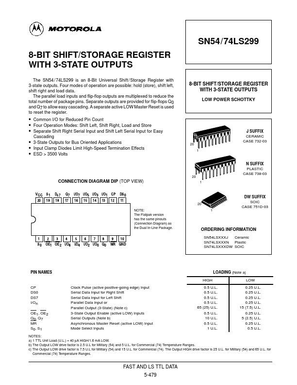
CONNECTION DIAGRAM DIP (TOP VIEW)
V CC 20 S 1 19 D s7 18 Q 7 17 I/O 7 16 I/O 5 15 I/O 3 14 I/O 1 13 CP 12 DS 0 11
20 NOTE: The Flatpak version has the same pinouts (Connection Diagram) as the Dual In-Line Package. 1
DW SUFFIX SOIC CASE 751D-03
ORDERING INFORMATION
SN54LSXXXJ Ceramic SN74LSXXXN Plastic SN74LSXXXDW SOIC
1 S 0
2 OE 1
3 OE 2
4 I/O 6
5 I/O 4
6 I/O 2
7 I/O 0
8 Q 0
9 MR
10 GND
PIN NAMES HIGH CP DS0 DS7 I/On OE1, OE2 Q0, Q7 MR S0, S1 Clock Pulse (active positive-going edge) Input Serial Data Input for Right Shift Serial Data I...
Similar Datasheet