Product Folder
Sample & Buy
Technical Documents
Tools & Software
Support & Community
SN74LV125A
SCES124N – DECEMBER...
Product Folder
Sample & Buy
Technical Documents
Tools & Software
Support & Community
SN74LV125A
SCES124N – DECEMBER 1997 – REVISED JANUARY 2016
SN74LV125A Quadruple Bus Buffer Gates With 3-State Outputs
1 Features
1 2-V to 5.5-V VCC Operation Max tpd of 6 ns at 5 V Typical VOLP (Output Ground Bounce)
< 0.8 V at VCC = 3.3 V, TA = 25°C Typical VOHV (Output VOH Undershoot)
> 2.3 V at VCC = 3.3 V, TA = 25°C Support Mixed-Mode
Voltage Operation on
All Ports
Ioff Supports Partial-Power-Down Mode Operation Latch-Up Performance Exceeds 250 mA Per
JESD 17
ESD Protection Exceeds JESD 22
– 4000-V Human-Body Model
– 200-V Machine Model
– 2000-V Charged-Device Model
2 Applications
Flow Meters Solid State Drives (SSDs): Enterprise Power Over Ethernet (PoE) Programmable Logic Controllers Motor Drives and Controls Electronic Points of Sale
3 Description
The SN74LV125A quadruple bus buffer gate is designed for 2-V to 5.5-V VCC operation.
Device Information(1)
PART NUMBER
PACKAGE
BODY SIZE (NOM)
TVSOP (14)
3.60 mm x 4.40 mm
SOIC (14)
8.65 mm × 3.91 mm
SN74LV125A
SOP (14)
10.30mm x 5.30 mm
SSOP (14)
6.20 mm x 5.30 mm
TSSOP (14)
5.00 mm x 4.40 mm
(1) For all available packages, see the orderable addendum at the end of the data sheet.
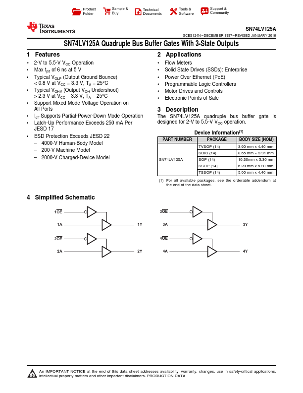
4 Simplified Schematic
1OE 1A
3OE 1Y 3A
3Y
2OE 2A
4OE 2Y 4A
4Y
1
An IMPORTANT NOTICE at the end of this data sheet addresses availability, warranty, changes, use in safety-critical applications, intellectual...