www.ti.com
FEATURES
• Inputs Are TTL-Voltage Compatible • 4.5-V to 5.5-V VCC Operation • Typical tpd of 3.8 ns at 5 V • ...
www.ti.com
FEATURES
Inputs Are TTL-
Voltage Compatible 4.5-V to 5.5-V VCC Operation Typical tpd of 3.8 ns at 5 V Typical VOLP (Output Ground Bounce)
<0.8 V at VCC = 5 V, TA = 25°C Typical VOHV (Output VOH Undershoot)
>2.3 V at VCC = 5 V, TA = 25°C Support Mixed-Mode
Voltage Operation on All
Ports
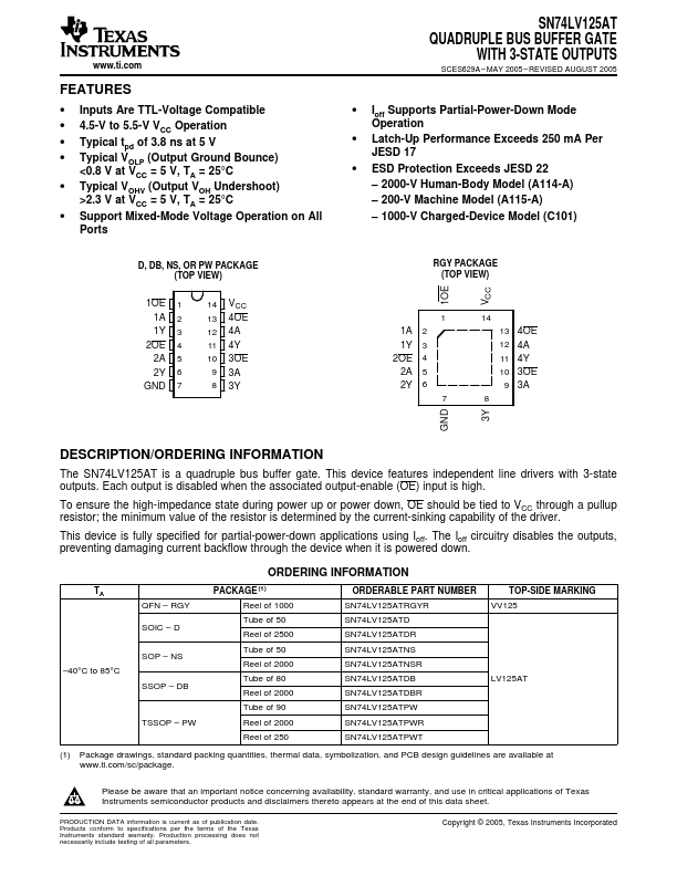
D, DB, NS, OR PW PACKAGE (TOP VIEW)
1OE 1A 1Y
2OE 2A 2Y
GND
1 2 3 4 5 6 7
14 VCC 13 4OE 12 4A 11 4Y 10 3OE 9 3A 8 3Y
SN74LV125AT QUADRUPLE BUS BUFFER GATE
WITH 3-STATE OUTPUTS
SCES629A – MAY 2005 – REVISED AUGUST 2005
Ioff Supports Partial-Power-Down Mode Operation
Latch-Up Performance Exceeds 250 mA Per JESD 17
ESD Protection Exceeds JESD 22 – 2000-V Human-Body Model (A114-A) – 200-V Machine Model (A115-A) – 1000-V Charged-Device Model (C101)
XXXX
XXXX
RGY PACKAGE (TOP VIEW)
1OE VCC
1A 1Y 2OE 2A 2Y
2 3 4 5 6
1 7
14 13 4OE 12 4A 11 4Y 10 3OE 9 3A
8
GND 3Y
DESCRIPTION/ORDERING INFORMATION
The SN74LV125AT is a quadruple bus buffer gate. This device features independent line drivers with 3-state outputs. Each output is disabled when the associated output-enable (OE) input is high.
To ensure the high-impedance state during power up or power down, OE should be tied to VCC through a pullup resistor; the minimum value of the resistor is determined by the current-sinking capability of the driver.
This device is fully specified for partial-power-down applications using Ioff. The Ioff circuitry disables the outputs, preventing damaging current backflow through the ...