Product Folder
Sample & Buy
Technical Documents
Tools & Software
Support & Community
SN54LV126A, SN74LV126A
SCES131...
Product Folder
Sample & Buy
Technical Documents
Tools & Software
Support & Community
SN54LV126A, SN74LV126A
SCES131I – MARCH 1998 – REVISED FEBRUARY 2015
SNx4LV126A Quadruple Bus Buffer Gates With 3-State Outputs
1 Features
1 2-V to 5.5-V VCC Operation Max tpd of 6.5 ns at 5 V Typical VOLP (Output Ground Bounce) <0.8 V at
VCC = 3.3 V, TA = 25°C Typical VOHV (Output VOH Undershoot) >2.3 V at
VCC = 3.3 V, TA = 25°C Ioff Supports Live Insertion, Partial Power Down
Mode, and Back Drive Protection Support Mixed-Mode
Voltage Operation on All
Ports Latch-Up Performance Exceeds 250 mA per
JESD 17 ESD Protection Exceeds JESD 22
– 2000-V Human-Body Model (A114-A) – 200-V Machine Model (A115-A) – 1000-V Charged-Device Model (C101)
2 Applications
Servers Network Switch Electronic Point of Sales TV Set-Top-Box
3 Description
The ‘LV126A quadruple bus buffer gates are designed for 2-V to 5.5-V VCC operation.
These quadruple bus buffer gates are designed for 2V to 5.5-V VCC operation.
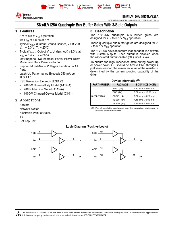
The ’LV126A devices feature independent line drivers with 3-state outputs. Each output is disabled when the associated output-enable (OE) input is low.
To ensure the high-impedance state during power up or power down, OE should be tied to GND through a pulldown resistor; the minimum value of the resistor is determined by the current-sourcing capability of the driver.
Device Information(1)
PART NUMBER
PACKAGE
BODY SIZE (NOM)
SOIC (14)
3.91 mm × 8.65 mm
SOP (14)
5.30 mm × 1...