D 2-V to 5.5-V VCC Operation D Max tpd of 8.5 ns at 5 V D Typical VOLP (Output Ground Bounce)
<0.8 V at VCC = 3.3 V, TA ...
D 2-V to 5.5-V VCC Operation D Max tpd of 8.5 ns at 5 V D Typical VOLP (Output Ground Bounce)
<0.8 V at VCC = 3.3 V, TA = 25°C
D Typical VOHV (Output VOH Undershoot)
>2.3 V at VCC = 3.3 V, TA = 25°C
D Support Mixed-Mode
Voltage Operation on
All Ports
D Latch-Up Performance Exceeds 250 mA Per
JESD 17
D ESD Protection Exceeds JESD 22
− 2000-V Human-Body Model (A114-A)
− 200-V Machine Model (A115-A)
− 1000-V Charged-Device Model (C101)
SN54LV174A, SN74LV174A HEX DĆTYPE FLIPĆFLOPS WITH CLEAR
SCLS401G − APRIL 1998 − REVISED APRIL 2005
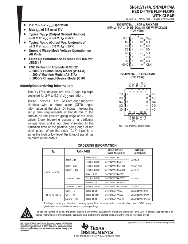
SN54LV174A . . . J OR W PACKAGE SN74LV174A . . . D, DB, DGV, NS, OR PW PACKAGE
(TOP VIEW)
CLR 1 1Q 2 1D 3 2D 4 2Q 5 3D 6 3Q 7
GND 8
16 VCC 15 6Q 14 6D 13 5D 12 5Q 11 4D 10 4Q 9 CLK
SN54LV174A . . . FK PACKAGE (TOP VIEW)
1Q CLR NC VCC 6Q
description/ordering information
The ’LV174A devices are hex D-type flip-flops designed for 2-V to 5.5-V VCC operation.
These devices are positive-edge-triggered flip-flops with a direct clear (CLR) input. Information at the data (D) inputs meeting the setup time requirements is transferred to the outputs on the positive-going edge of the clock pulse. Clock triggering occurs at a particular
voltage level and is not directly related to the transition time of the positive-going edge of the clock pulse. When the clock (CLK) input is at either the high or low level, the D-input signal has no effect at the output.
3 2 1 20 19
1D 4
18 6D
2D 5
17 5D
NC 6
16 NC
2Q 7
15 5Q
3D 8
14 4D
9 10 11 12 13
3Q GND
NC ...