SN74LV1T34
SCLS743E – DECEMBER 2013 – REVISED FEBRUARY 2024
SN74LV1T34 Single Power Supply Single Buffer GATE CMOS Logic...
SN74LV1T34
SCLS743E – DECEMBER 2013 – REVISED FEBRUARY 2024
SN74LV1T34 Single Power Supply Single Buffer GATE
CMOS Logic Level Shifter
1 Features
Latch-up performance exceeds 250mA per JESD 17
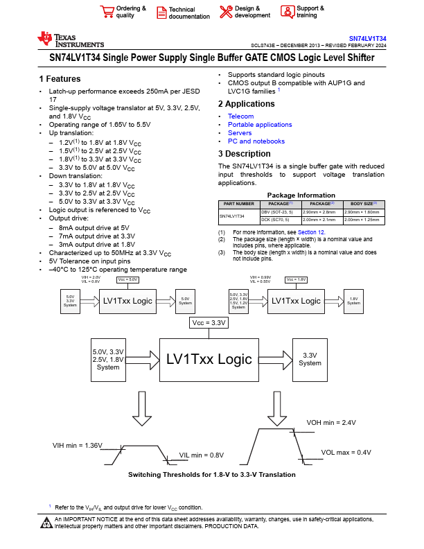
Single-supply
voltage translator at 5V, 3.3V, 2.5V, and 1.8V VCC
Operating range of 1.65V to 5.5V Up translation:
– 1.2V(1) to 1.8V at 1.8V VCC – 1.5V(1) to 2.5V at 2.5V VCC – 1.8V(1) to 3.3V at 3.3V VCC – 3.3V to 5.0V at 5.0V VCC Down translation:
– 3.3V to 1.8V at 1.8V VCC – 3.3V to 2.5V at 2.5V VCC – 5.0V to 3.3V at 3.3V VCC Logic output is referenced to VCC Output drive:
– 8mA output drive at 5V – 7mA output drive at 3.3V – 3mA output drive at 1.8V Characterized up to 50MHz at 3.3V VCC 5V Tolerance on input pins –40°C to 125°C operating temperature range
VIH = 2.0V VIL = 0.8V
Vcc = 5.0V
5.0V 3.3V System
LV1Txx Logic
5.0V System
Supports standard logic pinouts
CMOS output B compatible with AUP1G and
LVC1G families 1
2 Applications
Telecom Portable applications Servers PC and notebooks
3 Description
The SN74LV1T34 is a single buffer gate with reduced input thresholds to support
voltage translation applications.
PART NUMBER SN74LV1T34
Package Information
PACKAGE(1)
PACKAGE(2)
DBV (SOT-23, 5) 2.90mm × 2.8mm
DCK (SC70, 5)
2.00mm × 2.1mm
BODY SIZE(3) 2.90mm × 1.60mm 2.00mm × 1.25mm
(1) For more information, see Section 12. (2) The package size (length × width) is a nominal value and
includes pins, where applicable. (3) The body size (leng...