www.ti.com
FEATURES
• Inputs Are TTL-Voltage Compatible • 4.5-V to 5.5-V VCC Operation • Typical tpd = 5.4 ns at 5 V • T...
www.ti.com
FEATURES
Inputs Are TTL-
Voltage Compatible 4.5-V to 5.5-V VCC Operation Typical tpd = 5.4 ns at 5 V Typical VOLP (Output Ground Bounce)
<0.8 V at VCC = 5 V, TA = 25°C Typical VOHV (Output VOH Undershoot)
>2.3 V at VCC = 5 V, TA = 25°C Supports Mixed-Mode
Voltage Operation on
All Ports
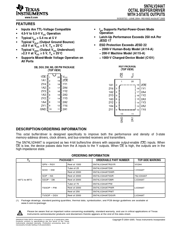
DB, DGV, DW, NS, OR PW PACKAGE (TOP VIEW)
1OE 1A1 2Y4 1A2 2Y3 1A3 2Y2 1A4 2Y1 GND
1 2 3 4 5 6 7 8 9 10
20 VCC 19 2OE 18 1Y1 17 2A4 16 1Y2 15 2A3 14 1Y3 13 2A2 12 1Y4 11 2A1
SN74LV244AT OCTAL BUFFER/DRIVER WITH 3-STATE OUTPUTS
SCES572C – JUNE 2004 – REVISED AUGUST 2005
Ioff Supports Partial-Power-Down Mode Operation
Latch-Up Performance Exceeds 250 mA Per JESD 17
ESD Protection Exceeds JESD 22 – 2000-V Human-Body Model (A114-A) – 200-V Machine Model (A115-A) – 1000-V Charged-Device Model (C101)
RGY PACKAGE (TOP VIEW)
1OE VCC
1A1 2 2Y4 3 1A2 4 2Y3 5 1A3 6 2Y2 7 1A4 8 2Y1 9
1 10
20 19 2OE 18 1Y1 17 2A4 16 1Y2 15 2A3 14 1Y3 13 2A2 12 1Y4
11
GND 2A1
DESCRIPTION/ORDERING INFORMATION
This octal buffer/driver is designed specifically to improve both the performance and density of 3-state memory-address drivers, clock drivers, and bus-oriented receivers and transmitters.
The SN74LV244AT is organized as two 4-bit buffers/line drivers with separate output-enable (OE) inputs. When OE is low, the device passes data from the A inputs to the Y outputs. When OE is high, the outputs are in the high-impedance state.
TA –40°C to 85°C
ORDERING INFORMATION
PACKAGE (1)
ORDE...