SN74LV374A-Q1
OCTAL EDGE-TRIGGERED D-TYPE FLIP-FLOP
WITH 3-STATE OUTPUTS
SCLS468C − FEBRUARY 2003 − REVISED JANUARY 2008...
SN74LV374A-Q1
OCTAL EDGE-TRIGGERED D-TYPE FLIP-FLOP
WITH 3-STATE OUTPUTS
SCLS468C − FEBRUARY 2003 − REVISED JANUARY 2008
D Qualified for Automotive Applications
D Typical VOLP (Output Ground Bounce)
<0.8 V at VCC = 3.3 V, TA = 25°C
D Typical VOHV (Output VOH Undershoot)
>2.3 V at VCC = 3.3 V, TA = 25°C
D Supports Mixed-Mode
Voltage Operation on
All Ports
D Ioff Supports Partial-Power-Down Mode
Operation
D ESD Protection Exceeds JESD 22
− 2000-V Human-Body Model (A114-A) − 200-V Machine Model (A115-A) − 1000-V Charged-Device Model (C101)
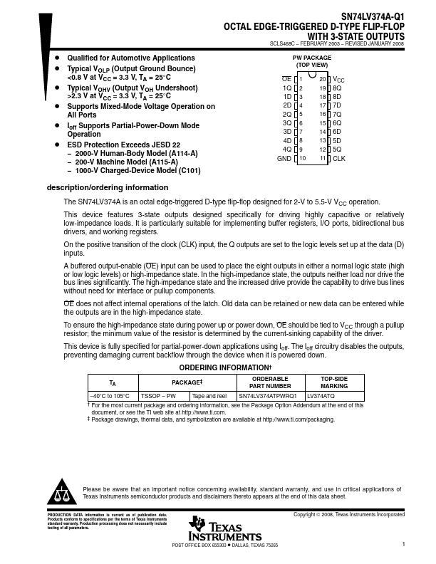
PW PACKAGE (TOP VIEW)
OE 1 1Q 2 1D 3 2D 4 2Q 5 3Q 6 3D 7 4D 8 4Q 9 GND 10
20 VCC 19 8Q 18 8D 17 7D 16 7Q 15 6Q 14 6D 13 5D 12 5Q 11 CLK
description/ordering information
The SN74LV374A is an octal edge-triggered D-type flip-flop designed for 2-V to 5.5-V VCC operation.
This device features 3-state outputs designed specifically for driving highly capacitive or relatively low-impedance loads. It is particularly suitable for implementing buffer registers, I/O ports, bidirectional bus drivers, and working registers.
On the positive transition of the clock (CLK) input, the Q outputs are set to the logic levels set up at the data (D) inputs.
A buffered output-enable (OE) input can be used to place the eight outputs in either a normal logic state (high or low logic levels) or high-impedance state. In the high-impedance state, the outputs neither load nor drive the bus lines significantly. The high-impedance state and the increased drive provid...