Product Folder
Sample & Buy
Technical Documents
Tools & Software
Support & Community
SN74LV540A
SCLS409I – MAY 1998...
Product Folder
Sample & Buy
Technical Documents
Tools & Software
Support & Community
SN74LV540A
SCLS409I – MAY 1998 – REVISED DECEMBER 2014
SN74LV540A Octal Buffers/Drivers with 3-State Outputs
1 Features
1 2-V to 5.5-V VCC Operation Max tpd of 8.5 ns at 5 V Typical VOLP (Output Ground Bounce)
< 0.8 V at VCC = 3.3 V, TA = 25°C Typical VOHV (Output VOH Undershoot)
> 2.3 V at VCC = 3.3 V, TA = 25°C Support Mixed-Mode
Voltage Operation on
All Ports
Ioff Supports Partial-Power-Down Mode Operation Latch-Up Performance Exceeds 250 mA
Per JESD 17
ESD Protection Exceeds JESD 22
– 2000-V Human-Body Model
– 200-V Machine Model
– 2000-V Charged-Device Model
2 Applications
Tests and Measurements Industrial Transports Patient Monitoring Wireless Infrastructure Network Switches Automotive Infotainment
3 Description
The SN74LV540A device is an octal buffer/driver designed for 2-V to 5.5-V VCC operation.
This device is ideal for driving bus lines or buffer memory address registers. It features inputs and outputs on opposite sides of the package to facilitate printed circuit board layout.
Device Information(1)
PART NUMBER
PACKAGE
BODY SIZE (NOM)
VQFN (20)
4.50 x 3.50 mm
SSOP (20)
7.50 x 5.30 mm
SN74LV540A
TSSOP (20)
6.50 x 4.40 mm
TVSOP (20)
5.00 x 4.40 mm
SOIC (20)
12.80 x 7.50 mm
(1) For all available packages, see the orderable addendum at the end of the data sheet.
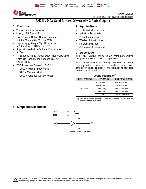
4 Simplified Schematic
OE1 OE2
A1 Y1
To Seven Other Channels
1
An IMP...