Product Folder
Sample & Buy
Technical Documents
Tools & Software
Support & Community
SN74LV595A
SCLS414Q – APRIL 19...
Product Folder
Sample & Buy
Technical Documents
Tools & Software
Support & Community
SN74LV595A
SCLS414Q – APRIL 1998 – REVISED APRIL 2016
SN74LV595A 8-Bit Shift Registers With 3-State Output Registers
1 Features
1 2-V to 5.5-V VCC Operation Max tpd of 7.1 ns at 5 V Typical VOLP (Output Ground Bounce)
< 0.8 V at VCC = 3.3 V, TA = 25°C Typical VOHV (Output VOH Undershoot)
> 2.3 V at VCC = 3.3 V, TA = 25°C Support Mixed-Mode
Voltage Operation on All
Ports
8-Bit Serial-In, Parallel-Out Shift
Ioff Supports Live Insertion, Partial Power-Down Mode, and Back-Drive Protection
Shift Register Has Direct Clear
Latch-Up Performance Exceeds 250 mA Per JESD 17
ESD Protection Exceeds JESD 22
– 2000-V Human-Body Model
– 200-V Machine Model
– 1000-V Charged-Device Model
2 Applications
Network Switches Power Infrastructures PCs and Notebooks LED Displays Servers I/O Expanders
3 Description
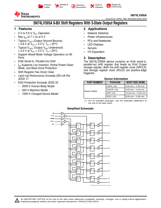
The SN74LV595A device contains an 8-bit serial-in, parallel-out shift register that feeds an 8-bit D-type storage register. Both the shift register clock (SRCLK) and storage register clock (RCLK) are positive-edge triggered.
Device Information
PART NUMBER
PACKAGE
BODY SIZE (NOM)
VQFN (16)
4.00 mm × 3.50 mm
SNx4LV595A
TSSOP (16) SOP (16)
5.00 mm × 4.40 mm 10.20 mm × 5.30 mm
SOIC (16)
9.00 mm × 3.90 mm
(1) For all available packages, see the orderable addendum at the end of the data sheet.
OE RCLK SRCLR SRCLK
SER
Simplified Schematic
1D Q C1
R
3D C3 Q
QA
...