SN74LVC126A-Q1
www.ti.com ................................................................................................
SN74LVC126A-Q1
www.ti.com .................................................................................................................................................. SCAS763B – FEBRUARY 2004 – REVISED APRIL 2008
QUADRUPLE BUS BUFFER GATE WITH 3-STATE OUTPUTS
FEATURES
1
Qualified for Automotive Applications Operates From 1.65 V to 3.6 V Inputs Accept
Voltages to 5.5 V Max tpd of 4.7 ns at 3.3 V Typical VOLP (Output Ground Bounce) <0.8 V at
VCC = 3.3 V, TA = 25°C Typical VOHV (Output VOH Undershoot) >2 V at
VCC = 3.3 V, TA = 25°C Latch-Up Performance Exceeds 250 mA Per
JESD 17
ESD Protection Exceeds JESD 22 – 2000-V Human-Body Model (A114-A)
– 200-V Machine Model (A115-A)
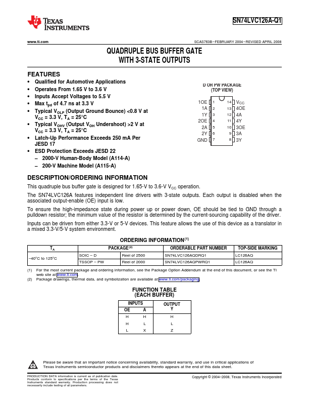
D OR PW PACKAGE (TOP VIEW)
1OE 1 1A 2 1Y 3
2OE 4 2A 5 2Y 6
GND 7
14 VCC 13 4OE 12 4A 11 4Y 10 3OE 9 3A 8 3Y
DESCRIPTION/ORDERING INFORMATION
This quadruple bus buffer gate is designed for 1.65-V to 3.6-V VCC operation.
The SN74LVC126A features independent line drivers with 3-state outputs. Each output is disabled when the associated output-enable (OE) input is low.
To ensure the high-impedance state during power up or power down, OE should be tied to GND through a pulldown resistor; the minimum value of the resistor is determined by the current-sourcing capability of the driver.
Inputs can be driven from either 3.3-V or 5-V devices. This feature allows the use of this device as a translator in a mixed 3.3-V/5-V system environment.
TA –40°C to 125°C
ORDERING INFORMATION(1)
PACKAG...