SN74LVC1G04-EP
www.ti.com ................................................................................................
SN74LVC1G04-EP
www.ti.com ................................................................................................................................................. SCES691A – MARCH 2007 – REVISED OCTOBER 2008
SINGLE INVERTER GATE
FEATURES
1
2 Supports 5-V VCC Operation Inputs Accept
Voltages to 5.5 V Max tpd of 3.3 ns at 3.3 V Low Power Consumption, 10-µA Max ICC ±24-mA Output Drive at 3.3 V Ioff Supports Partial-Power-Down Mode
Operation Latch-Up Performance Exceeds 100 mA Per
JESD 78, Class II ESD Protection Exceeds JESD 22
– 2000-V Human-Body Model (A114-A)
– 200-V Machine Model (A115-A)
– 1000-V Charged-Device Model (C101)
SUPPORTS DEFENSE, AEROSPACE, AND MEDICAL APPLICATIONS
Controlled Baseline One Assembly/Test Site One Fabrication Site Available in Military (–55°C/125°C)
Temperature Range(1) Extended Product Life Cycle Extended Product-Change Notification Product Traceability
(1) Custom temperature ranges available
DESCRIPTION/ORDERING INFORMATION
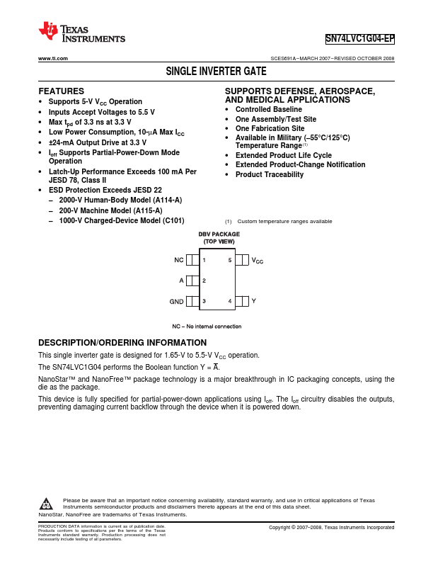
This single inverter gate is designed for 1.65-V to 5.5-V VCC operation. The SN74LVC1G04 performs the Boolean function Y = A.
NanoStar™ and NanoFree™ package technology is a major breakthrough in IC packaging concepts, using the die as the package.
This device is fully specified for partial-power-down applications using Ioff. The Ioff circuitry disables the outputs, preventing damaging current backflow through the device when it is powered down.
1
Please be aware that an important not...