SN74LVC1G04-Q1
www.ti.com
SCES482D – AUGUST 2003 – REVISED JANUARY 2013
SINGLE INVERTER GATE
Check for Samples: SN74LV...
SN74LVC1G04-Q1
www.ti.com
SCES482D – AUGUST 2003 – REVISED JANUARY 2013
SINGLE INVERTER GATE
Check for Samples: SN74LVC1G04-Q1
FEATURES
1
Qualified for Automotive Applications AEC-Q100 Qualified with the Following Results
– Device Temperature Grade 1: –40°C to 125°C Ambient Operating Temperature Range
– Device HBM ESD Classification Level H2 – Device CDM ESG Classification Level C4B ESD Protection Exceeds 2000 V Per MIL-STD883, Method 3015; Exceeds 200 V Using Machine Model (C = 200 pF, R = 0)
Supports 5-V VCC Operation Inputs Accept
Voltages to 5.5 V
Max tpd of 3.3 ns at 3.3 V Low Power Consumption, 10-μA Max ICC ±24-mA Output Drive at 3.3 V
Ioff Supports Partial-Power-Down Mode Operation
Latch-Up Performance Exceeds 100 mA Per JESD 78, Class II
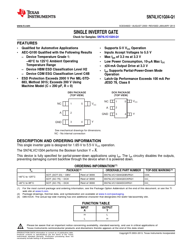
DBV PACKAGE (TOP VIEW)
DCK PACKAGE (TOP VIEW)
NC
1
A
2
NC
1
5
VCC
5
VCC
A
2
GND
3
4Y
GND
3
4
Y
See mechanical drawings for dimensions. NC - No internal connection
DESCRIPTION AND ORDERING INFORMATION
This single inverter gate is designed for 1.65-V to 5.5-V VCC operation.
The SN74LVC1G04 performs the Boolean function Y = A.
This device is fully specified for partial-power-down applications using Ioff. The Ioff circuitry disables the outputs, preventing damaging current backflow through the device when it is powered down.
TA –40°C to 125°C –40°C to 85°C
ORDERING INFORMATION(1)
PACKAGE (2)
ORDERABLE PART NUMBER
SOT (SOT-23) – DBV
Reel of 3000
SN74LVC1G04QDBVRQ1
SOT (SC-70) – DCK
R...