Product Folder
Sample & Buy
Technical Documents
Tools & Software
Support & Community
SN74LVC1G04
SCES214AD–APRIL199...
Product Folder
Sample & Buy
Technical Documents
Tools & Software
Support & Community
SN74LVC1G04
SCES214AD–APRIL1999–REVISED OCTOBER 2014
SN74LVC1G04 Single Inverter Gate
1 Features
1 Available in the Ultra-Small 0.64-mm2 Package (DPW) with 0.5-mm Pitch
Supports 5-V VCC Operation Inputs Accept
Voltages up to 5.5 V Allowing Down
Translation to VCC Max tpd of 3.3 ns at 3.3-V Low Power Consumption, 10-μA Max ICC ±24-mA Output Drive at 3.3-V Ioff Supports Live-Insertion, Partial-Power-Down
Mode, and Back-Drive Protection Latch-Up Performance Exceeds 100 mA
Per JESD 78, Class II ESD Protection Exceeds JESD 22
– 2000-V Human-Body Model (A114-A) – 200-V Machine Model (A115-A) – 1000-V Charged-Device Model (C101)
2 Applications
AV Receiver Audio Dock: Portable Blu-ray Player and Home Theater Embedded PC MP3 Player/Recorder (Portable Audio) Personal Digital Assistant (PDA) Power: Telecom/Server AC/DC Supply: Single
Controller: Analog and Digital Solid State Drive (SSD): Client and Enterprise TV: LCD/Digital and High-Definition (HDTV) Tablet: Enterprise Video Analytics: Server Wireless Headset, Keyboard, and Mouse
3 Description
This single inverter gate is designed for 1.65-V to 5.5-V VCC operation.
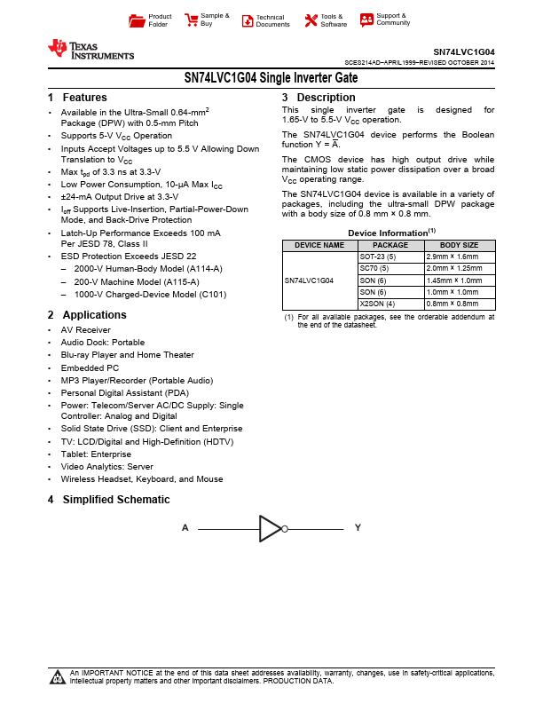
The SN74LVC1G04 device performs the Boolean function Y = A.
The
CMOS device has high output drive while maintaining low static power dissipation over a broad VCC operating range.
The SN74LVC1G04 device is available in a variety of packages, in...