SN74LVC1G0832
www.ti.com
SCES606D – SEPTEMBER 2004 – REVISED DECEMBER 2013
Single 3-Input Positive AND-OR Gate
Check ...
SN74LVC1G0832
www.ti.com
SCES606D – SEPTEMBER 2004 – REVISED DECEMBER 2013
Single 3-Input Positive AND-OR Gate
Check for Samples: SN74LVC1G0832
FEATURES
1
2 Available in the Texas Instruments NanoFree™ Package
Supports 5-V VCC Operation Inputs Accept
Voltages to 5.5 V Provides Down Translation to VCC Max tpd of 5 ns at 3.3 V Low Power Consumption, 10-µA Max ICC ±24-mA Output Drive at 3.3 V Input Hysteresis Allows Slow Input
Transition and Better Switching Noise Immunity at the Input (Vhys = 250 mV Typ @ 3.3 V) Can Be Used in Three Combinations: – AND-OR Gate – AND Gate – OR Gate Ioff Supports Live Insertion, Partial-PowerDown Mode, and Back-Drive Protection Latch-Up Performance Exceeds 100 mA Per JESD 78, Class II ESD Protection Exceeds JESD 22 – 2000-V Human-Body Model (A114-A) – 200-V Machine Model (A115-A) – 1000-V Charged-Device Model (C101)
DESCRIPTION
This device is designed for 1.65-V to 5.5-V VCC operation.
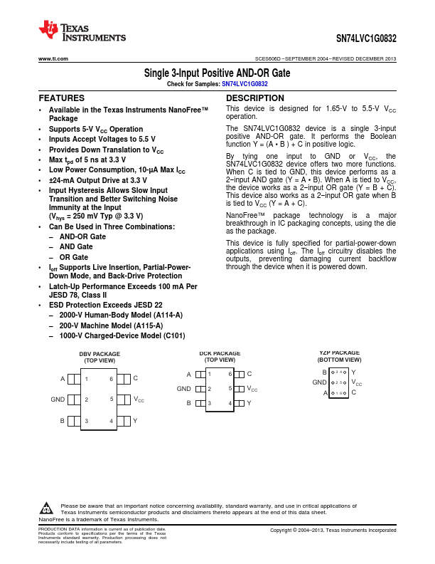
The SN74LVC1G0832 device is a single 3-input positive AND-OR gate. It performs the Boolean function Y = (A B ) + C in positive logic.
By tying one input to GND or VCC, the SN74LVC1G0832 device offers two more functions. When C is tied to GND, this device performs as a 2−input AND gate (Y = A B). When A is tied to VCC, the device works as a 2−input OR gate (Y = B + C). This device also works as a 2−input OR gate when B is tied to VCC (Y = A + C).
NanoFree™ package technology is a major breakthrough in IC packaging concepts, using the ...