SN74LVC1G3208-Q1
www.ti.com
SINGLE 3-INPUT POSITIVE OR-AND GATE
Check for Samples: SN74LVC1G3208-Q1
SCES822 – DECEMBE...
SN74LVC1G3208-Q1
www.ti.com
SINGLE 3-INPUT POSITIVE OR-AND GATE
Check for Samples: SN74LVC1G3208-Q1
SCES822 – DECEMBER 2010
FEATURES
1
Qualified for Automotive Applications
Supports 5-V VCC Operation Inputs Accept
Voltages to 5.5 V
Max tpd of 5 ns at 3.3 V Low Power Consumption, 10-mA Max ICC ±24-mA Output Drive at 3.3 V
Input Hysteresis Allows Slow Input Transition and Better Switching Noise Immunity at the Input (Vhys = 250 mV Typ at 3.3 V)
Can Be Used in Three Combinations:
– OR-AND Gate
– OR Gate
– AND Gate
Ioff Supports Partial-Power-Down Mode Operation
DESCRIPTION/ORDERING INFORMATION
This device is designed for 1.65-V to 5.5-V VCC operation.
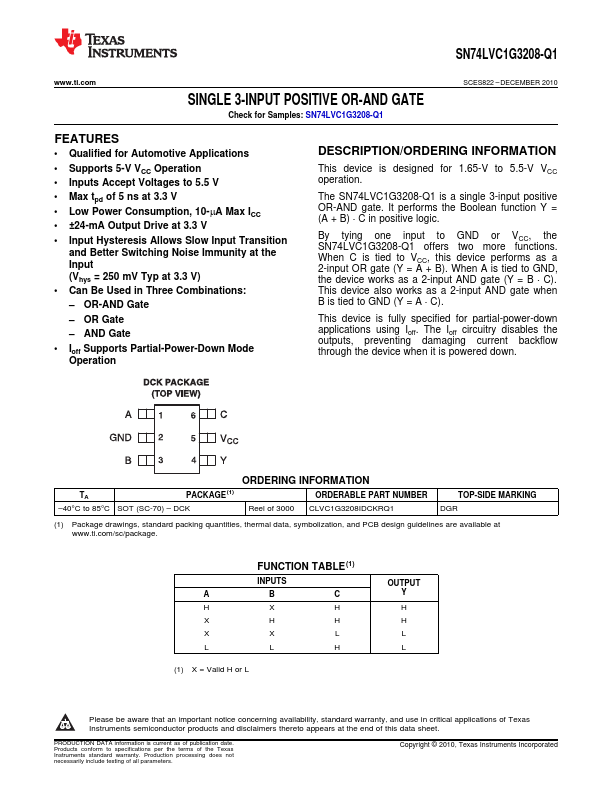
The SN74LVC1G3208-Q1 is a single 3-input positive OR-AND gate. It performs the Boolean function Y = (A + B) ⋅ C in positive logic.
By tying one input to GND or VCC, the SN74LVC1G3208-Q1 offers two more functions. When C is tied to VCC, this device performs as a 2-input OR gate (Y = A + B). When A is tied to GND, the device works as a 2-input AND gate (Y = B ⋅ C). This device also works as a 2-input AND gate when B is tied to GND (Y = A ⋅ C).
This device is fully specified for partial-power-down applications using Ioff. The Ioff circuitry disables the outputs, preventing damaging current backflow through the device when it is powered down.
TA –40°C to 85°C
PACKAGE (1) SOT (SC-70) – DCK
ORDERING INFORMATION
ORDERABLE PART NUMBER Reel of 3000 CLVC1G3208IDCKRQ1
TOP-SIDE MARKING DGR
(1) Package drawings, stan...