SN74LVC1G332
www.ti.com
SCES489E – SEPTEMBER 2003 – REVISED DECEMBER 2013
Single 3-Input Positive-OR Gate
Check for S...
SN74LVC1G332
www.ti.com
SCES489E – SEPTEMBER 2003 – REVISED DECEMBER 2013
Single 3-Input Positive-OR Gate
Check for Samples: SN74LVC1G332
FEATURES
1
2 Available in the Texas Instruments NanoStar™ and NanoFree™ Packages
Supports 5-V VCC Operation Inputs Accept
Voltages to 5.5 V Supports Down Translation to VCC Max tpd of 4.5 ns at 3.3 V Low Power Consumption, 10-µA Max ICC ±24-mA Output Drive at 3.3 V Ioff Supports Live Insertion, Partial-Power-
Down Mode, and Back-Drive Protection Latch-Up Performance Exceeds 100 mA Per
JESD 78, Class II ESD Protection Exceeds JESD 22
– 2000-V Human-Body Model (A114-A) – 200-V Machine Model (A115-A) – 1000-V Charged-Device Model (C101)
DESCRIPTION
The SN74LVC1G332 device performs the Boolean function in Y + A ) B ) C or Y + A B C positive logic.
NanoStar™ and NanoFree™ package technology is a major breakthrough in IC packaging concepts, using the die as the package.
This device is fully specified for partial-power-down applications using Ioff. The Ioff circuitry disables the outputs, preventing damaging current backflow through the device when it is powered down.
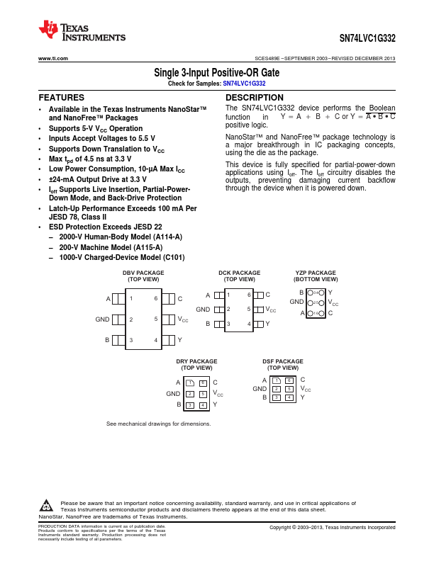
DBV PACKAGE (TOP VIEW)
A1
6
GND
2
5
DCK PACKAGE (TOP VIEW)
C A 1 6C GND 2 5 VCC
VCC B 3 4 Y
YZP PACKAGE (BOTTOM VIEW)
B GND
A
34 25 16
Y VCC C
B3 4Y
DRY PACKAGE (TOP VIEW)
A GND
B
1 2 3
6C 5 VCC 4Y
See mechanical drawings for dimensions.
DSF PACKAGE (TOP VIEW)
A1 6 C GND 2 5 VCC
B3 4 Y
1
Please be aware that an important notice concernin...