Product Folder
Sample & Buy
Technical Documents
Tools & Software
Support & Community
SN74LVC1G66-Q1
SCES499E – JUNE...
Product Folder
Sample & Buy
Technical Documents
Tools & Software
Support & Community
SN74LVC1G66-Q1
SCES499E – JUNE 2001 – REVISED APRIL 2015
SN74LVC1G66-Q1 Single Bilateral Analog Switch
1 Features
1 Qualified for Automotive Applications AEC-Q100 Qualified With the Following Results:
– Device Temperature Grade 1: –40°C to 125°C Ambient Operating Temperature Range
– Device HBM Classification Level H2 – Device CDM Classification Level C5 – Device MM Classification Level M3 1.65-V to 5.5-V VCC Operation Inputs Accept
Voltages to 5.5 V Max tpd of 0.8 ns at 3.3 V High On-Off Output
Voltage Ratio High Degree of Linearity High Speed, Typically 0.5 ns (VCC = 3 V, CL = 50 pF) Low ON-State Resistance, Typically ≉5.5 Ω (VCC = 4.5 V) Latch-Up Performance Exceeds 100 mA Per JESD 78, Class II
2 Applications
Infotainment Systems Wireless Devices Audio and Video Signal Routing Portable Computing Wearable Devices Signal Gating, Chopping, Modulation or
Demodulation (Modem) Signal Multiplexing for Analog-to-Digital and
Digital-to-Analog Conversion Systems
3 Description
This single analog switch is designed for 1.65-V to 5.5-V VCC operation.
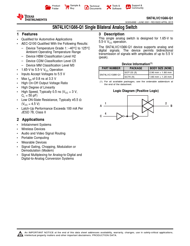
The SN74LVC1G66-Q1 device supports analog and digital signals. The device permits bidirectional transmission of signals with amplitudes of up to 5.5 V (peak).
Device Information(1)
PART NUMBER
PACKAGE
BODY SIZE (NOM)
SOT-23 (5) SN74LVC1G66-Q1
SC70 (5)
2.90 mm × 1.60 mm 1.60 mm × 1.20 mm
(1) For all available pa...