SN74LVC1G99
www.ti.com
SCES609G – SEPTEMBER 2004 – REVISED NOVEMBER 2013
Ultra-Configurable Multiple-Function Gate Wit...
SN74LVC1G99
www.ti.com
SCES609G – SEPTEMBER 2004 – REVISED NOVEMBER 2013
Ultra-Configurable Multiple-Function Gate With 3-State Output
Check for Samples: SN74LVC1G99
FEATURES
1
2 Available in Texas Instruments NanoFree™ Package
Supports 5-V VCC Operation Inputs Accept
Voltages to 5.5 V Supports Down Translation to VCC Max tpd of 6.7 ns at 3.3 V Low Power Consumption, 10-µA Max ICC ±24-mA Output Drive at 3.3 V Offers Nine Different Logic Functions in a
Single Package Ioff Supports Live Insertion, Partial-Power-
Down Mode, and Back-Drive Protection Input Hysteresis Allows for Slow Input
Transition Time and Better Noise Immunity at Input Latch-Up Performance Exceeds 100 mA Per JESD 78, Class II ESD Protection Exceeds JESD 22 – 2000-V Human-Body Model (A114-A) – 200-V Machine Model (A115-A) – 1000-V Charged-Device Model (C101)
DESCRIPTION
The SN74LVC1G99 device is operational from 1.65 V to 5.5 V.
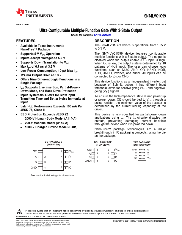
The SN74LVC1G99 device features configurable multiple functions with a 3-state output. The output is disabled when the output-enable (OE) input is high. When OE is low, the output state is determined by 16 patterns of 4-bit input. The user can choose logic functions, such as MUX, AND, OR, NAND, NOR, XOR, XNOR, inverter, and buffer. All inputs can be connected to VCC or GND.
This device functions as an independent inverter, but because of Schmitt action, it has different input threshold levels for positive-going (VT+) and negativegoing (VT–) signals.
To ensure ...