Product Folder
Sample & Buy
Technical Documents
Tools & Software
Support & Community
SN74LVC2G06
SCES307J – AUGUST ...
Product Folder
Sample & Buy
Technical Documents
Tools & Software
Support & Community
SN74LVC2G06
SCES307J – AUGUST 2001 – REVISED JULY 2015
SN74LVC2G06 Dual Inverter Buffer and Driver With Open-Drain Outputs
1 Features
1 Available in the Texas Instruments Package
Supports 5-V VCC Operation Max tpd of 3.4 ns at 3.3 V Low Power Consumption, 10-μA Max ICC ±24-mA Output Drive at 3.3 V
Typical VOLP (Output Ground Bounce) <0.8 V at VCC = 3.3 V, TA = 25°C
Typical VOHV (Output VOH Undershoot) >2 V at VCC = 3.3 V, TA = 25°C
Inputs and Open-Drain Outputs Accept
Voltages up to 5.5 V
Ioff Supports Live Insertion, Partial-Power-Down Mode and Back-Drive Protection
Latch-Up Performance Exceeds 100 mA Per JESD 78, Class II
Supports Down-Translation (5 V to 3.3 V and 3.3 V to 1.8 V)
ESD Protection Exceeds JESD 22
– 2000-V Human Body Model (A114-A)
– 200-V Machine Model (A115-A)
– 1000-V Charged-Device Model (C101)
3 Description
This dual inverter buffer and driver is designed for 1.65-V to 5.5-V VCC operation.
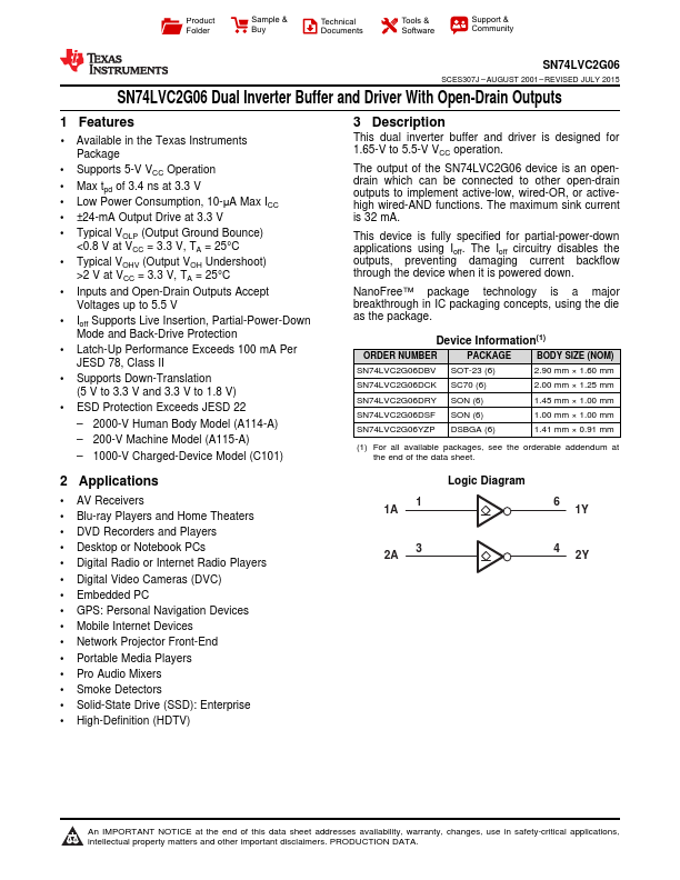
The output of the SN74LVC2G06 device is an opendrain which can be connected to other open-drain outputs to implement active-low, wired-OR, or activehigh wired-AND functions. The maximum sink current is 32 mA.
This device is fully specified for partial-power-down applications using Ioff. The Ioff circuitry disables the outputs, preventing damaging current backflow through the device when it is powered down.
NanoFree™ package technology is a major breakthroug...