Product Folder
Sample & Buy
Technical Documents
Tools & Software
Support & Community
SN74LVC2G126
SCES205M – APRIL ...
Product Folder
Sample & Buy
Technical Documents
Tools & Software
Support & Community
SN74LVC2G126
SCES205M – APRIL 1999 – REVISED SEPTEMBER 2016
SN74LVC2G126 Dual Bus Buffer Gate With 3-State Outputs
1 Features
1 Available in the Texas Instruments NanoFree™ Package
Supports 5-V VCC Operation Inputs Accept
Voltages to 5.5 V
Max tpd of 4ns at 3.3V Low Power Consumption, 10-µA Max ICC ±24-mA Output Drive at 3.3 V
Typical VOLP (Output Ground Bounce) < 0.8 V at VCC = 3.3 V, TA = 25°C
Typical VOHV (Output VOH Undershoot) > 2 V at VCC = 3.3 V, TA = 25°C
Ioff Supports Live Insertion, Partial-Power-Down Mode, and Back-Drive Protection
Can Be Used as a Down Translator to Translate Inputs From a Max of 5.5 V Down to the VCC Level
Latch-Up Performance Exceeds 100 mA Per JESD 78, Class II
ESD Protection Exceeds JESD 22
– 2000-V Human-Body Model
– 1000-V Charged-Device Model
2 Applications
Cable Modem Termination Systems High-Speed Data Acquisition and Generation Military: Radars and Sonars Motor Controls: High-
Voltage Power Line Communication Modems SSDs: Internal or External Video Broadcasting and Infrastructure: Scalable
Platforms Video Broadcasting: IP-Based Multi-Format
Transcoders Video Communication Systems
3 Description
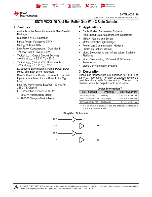
These bus transceivers are designed for 1.65-V to 3.6-V VCC operation. The SN74LVC2G126 device is a dual line driver with 3-state output. The output is disabled when the output-enable input is low.
Device Information...