Product Folder
Order Now
Technical Documents
Tools & Software
Support & Community
SN74LVC2G66
SCES325N – JULY 2001 ...
Product Folder
Order Now
Technical Documents
Tools & Software
Support & Community
SN74LVC2G66
SCES325N – JULY 2001 – REVISED AUGUST 2018
SN74LVC2G66 Dual Bilateral Analog Switch
1 Features
1 Available in the Texas Instruments NanoFree™ Package
1.65-V to 5.5-V VCC Operation Inputs Accept
Voltages to 5.5 V Max tpd of 0.8 ns at 3.3 V High On-Off Output
Voltage Ratio High Degree of Linearity High Speed, Typically 0.5 ns
(VCC = 3 V, CL = 50 pF) Rail-to-Rail Input/Output Low ON-State Resistance, Typically ≉6 Ω
(VCC = 4.5 V) Latch-Up Performance Exceeds 100 mA Per
JESD 78, Class II
2 Applications
Wireless Devices Audio and Video Signal Routing Portable Computing Wearable Devices Signal Gating, Chopping, Modulation or
Demodulation (Modem) Signal Multiplexing for Analog-to-Digital and
Digital-to-Analog Conversion Systems
3 Description
This dual bilateral analog switch is designed for 1.65-V to 5.5-V VCC operation.
The SN74LVC2G66 device can handle both analog and digital signals. The SN74LVC2G66 device permits signals with amplitudes of up to 5.5 V (peak) to be transmitted in either direction.
NanoFree package technology is a major breakthrough in IC packaging concepts, using the die as the package.
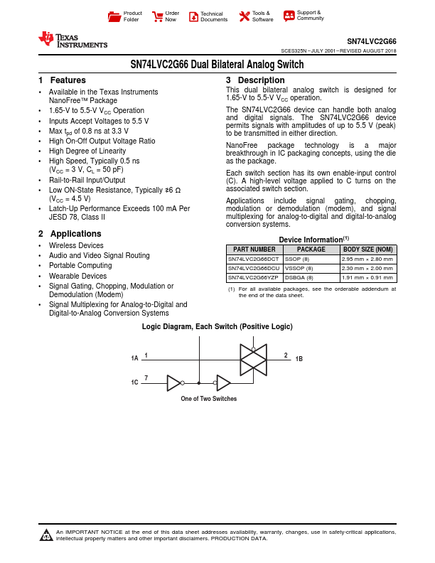
Each switch section has its own enable-input control (C). A high-level
voltage applied to C turns on the associated switch section.
Applications include signal gating, chopping, modulation or demodulation (modem), and signal multiplexing for analog-to-...