SN74LVC2G80
www.ti.com
SCES309F – DECEMBER 2001 – REVISED DECEMBER 2013
Dual Positive-Edge-Triggered D-Type Flip-Flop
...
SN74LVC2G80
www.ti.com
SCES309F – DECEMBER 2001 – REVISED DECEMBER 2013
Dual Positive-Edge-Triggered D-Type Flip-Flop
Check for Samples: SN74LVC2G80
FEATURES
1
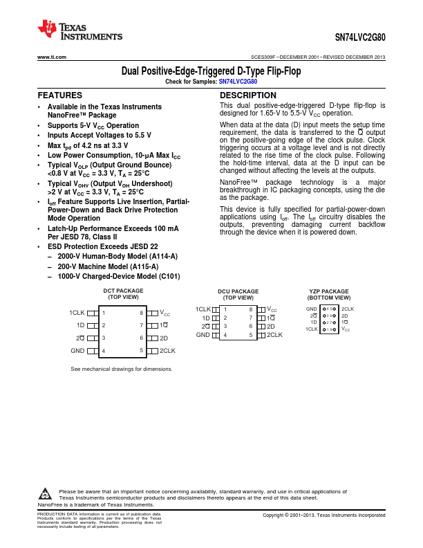
2 Available in the Texas Instruments NanoFree™ Package
Supports 5-V VCC Operation Inputs Accept
Voltages to 5.5 V
Max tpd of 4.2 ns at 3.3 V Low Power Consumption, 10-μA Max ICC Typical VOLP (Output Ground Bounce)
<0.8 V at VCC = 3.3 V, TA = 25°C Typical VOHV (Output VOH Undershoot)
>2 V at VCC = 3.3 V, TA = 25°C Ioff Feature Supports Live Insertion, Partial-
Power-Down and Back Drive Protection Mode Operation
Latch-Up Performance Exceeds 100 mA Per JESD 78, Class II
ESD Protection Exceeds JESD 22
– 2000-V Human-Body Model (A114-A)
– 200-V Machine Model (A115-A)
– 1000-V Charged-Device Model (C101)
DESCRIPTION
This dual positive-edge-triggered D-type flip-flop is designed for 1.65-V to 5.5-V VCC operation.
When data at the data (D) input meets the setup time requirement, the data is transferred to the Q output on the positive-going edge of the clock pulse. Clock triggering occurs at a
voltage level and is not directly related to the rise time of the clock pulse. Following the hold-time interval, data at the D input can be changed without affecting the levels at the outputs.
NanoFree™ package technology is a major breakthrough in IC packaging concepts, using the die as the package.
This device is fully specified for partial-power-down applications using Ioff. The Ioff circuitry disables the output...