SN74LVC2G86
www.ti.com
SCES360I – AUGUST 2001 – REVISED DECEMBER 2013
Dual 2-Input Exclusive-OR Gate
Check for Sample...
SN74LVC2G86
www.ti.com
SCES360I – AUGUST 2001 – REVISED DECEMBER 2013
Dual 2-Input Exclusive-OR Gate
Check for Samples: SN74LVC2G86
FEATURES
1
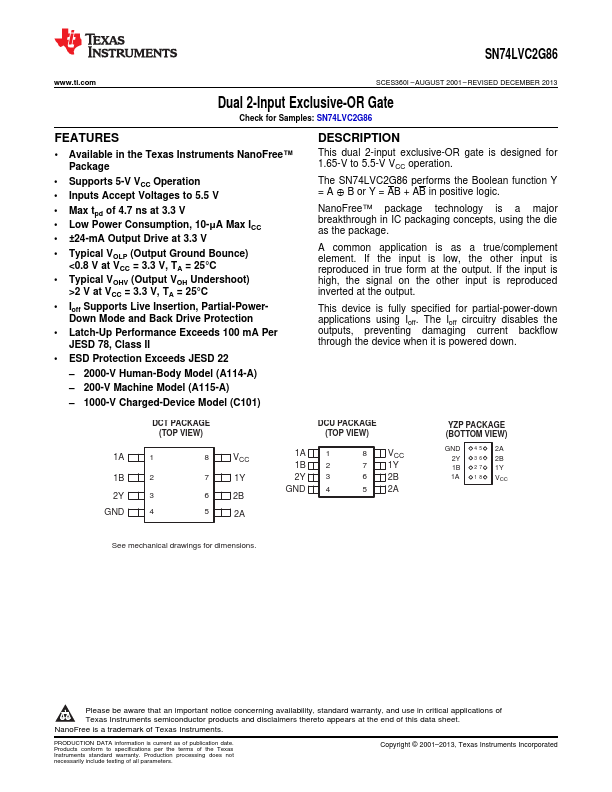
2 Available in the Texas Instruments NanoFree™ Package
Supports 5-V VCC Operation Inputs Accept
Voltages to 5.5 V
Max tpd of 4.7 ns at 3.3 V Low Power Consumption, 10-μA Max ICC ±24-mA Output Drive at 3.3 V
Typical VOLP (Output Ground Bounce) <0.8 V at VCC = 3.3 V, TA = 25°C
Typical VOHV (Output VOH Undershoot) >2 V at VCC = 3.3 V, TA = 25°C
Ioff Supports Live Insertion, Partial-PowerDown Mode and Back Drive Protection
Latch-Up Performance Exceeds 100 mA Per JESD 78, Class II
ESD Protection Exceeds JESD 22
– 2000-V Human-Body Model (A114-A)
– 200-V Machine Model (A115-A)
– 1000-V Charged-Device Model (C101)
DESCRIPTION
This dual 2-input exclusive-OR gate is designed for 1.65-V to 5.5-V VCC operation.
The SN74LVC2G86 performs the Boolean function Y = A ⊕ B or Y = AB + AB in positive logic.
NanoFree™ package technology is a major breakthrough in IC packaging concepts, using the die as the package.
A common application is as a true/complement element. If the input is low, the other input is reproduced in true form at the output. If the input is high, the signal on the other input is reproduced inverted at the output.
This device is fully specified for partial-power-down applications using Ioff. The Ioff circuitry disables the outputs, preventing damaging current backflow through the device when it is powered down...