www.ti.com
SN74LVC374A-Q1 OCTAL EDGE-TRIGGERED D-TYPE FLIP-FLOP
WITH 3-STATE OUTPUTS
SCAS711B – SEPTEMBER 2003 – REVISE...
www.ti.com
SN74LVC374A-Q1 OCTAL EDGE-TRIGGERED D-TYPE FLIP-FLOP
WITH 3-STATE OUTPUTS
SCAS711B – SEPTEMBER 2003 – REVISED FEBRUARY 2008
FEATURES
1
Qualified for Automotive Applications
ESD Protection Exceeds 2000 V Per MIL-STD-883, Method 3015; Exceeds 200 V Using Machine Model (C = 200 pF, R = 0)
Operates From 2 V to 3.6 V
Inputs Accept
Voltages to 5.5 V Max tpd of 8.5 ns at 3.3 V Typical VOLP (Output Ground Bounce) < 0.8 V
at VCC = 3.3 V, TA = 25°C Typical VOHV (Output VOH Undershoot) > 2 V
at VCC = 3.3 V, TA = 25°C Supports Mixed-Mode Signal Operation on All
Ports (5-V Input/Output
Voltage With 3.3-V VCC) Ioff Supports Partial-Power-Down Mode
Operation
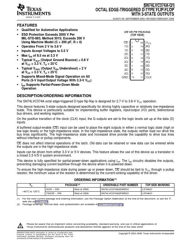
DW OR PW PACKAGE (TOP VIEW)
OE 1 1Q 2 1D 3 2D 4 2Q 5 3Q 6 3D 7 4D 8 4Q 9 GND 10
20 VCC 19 8Q 18 8D 17 7D 16 7Q 15 6Q 14 6D 13 5D 12 5Q 11 CLK
DESCRIPTION/ORDERING INFORMATION
The SN74LVC374A octal edge-triggered D-type flip-flop is designed for 2.7-V to 3.6-V VCC operation.
This device features 3-state outputs designed specifically for driving highly capacitive or relatively low-impedance loads. This device is particularly suitable for implementing buffer registers, input/output (I/O) ports, bidirectional bus drivers, and working registers.
On the positive transition of the clock (CLK) input, the Q outputs are set to the logic levels set up at the data (D) inputs.
A buffered output-enable (OE) input can be used to place the eight outputs in either a normal logic state (high or low logic levels) or the ...