SN54LVTH125, SN74LVTH125 3.3ĆV ABT QUADRUPLE BUS BUFFERS
WITH 3ĆSTATE OUTPUTS
SCBS703I − AUGUST 1997 − REVISED OCTOBER 2...
SN54LVTH125, SN74LVTH125 3.3ĆV ABT QUADRUPLE BUS BUFFERS
WITH 3ĆSTATE OUTPUTS
SCBS703I − AUGUST 1997 − REVISED OCTOBER 2003
D Support Mixed-Mode Signal Operation (5-V
Input and Output
Voltages With 3.3-V VCC)
D Support Unregulated Battery Operation
Down to 2.7 V
D Typical VOLP (Output Ground Bounce)
<0.8 V at VCC = 3.3 V, TA = 25°C
D Ioff and Power-Up 3-State Support Hot
Insertion
D Bus Hold on Data Inputs Eliminates the
Need for External Pullup/Pulldown Resistors
D Latch-Up Performance Exceeds 500 mA Per
JESD 17
D ESD Protection Exceeds JESD 22
− 2000-V Human-Body Model (A114-A) − 200-V Machine Model (A115-A)
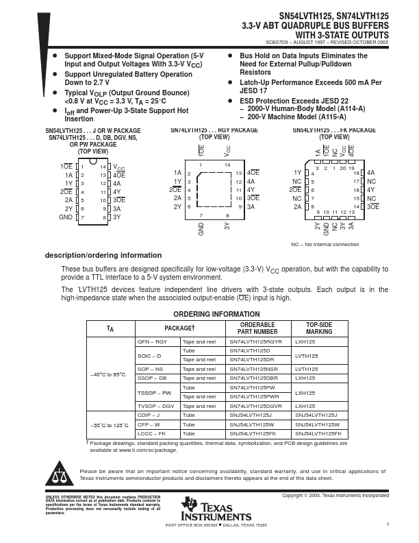
SN54LVTH125 . . . J OR W PACKAGE SN74LVTH125 . . . D, DB, DGV, NS, OR PW PACKAGE (TOP VIEW)
SN74LVTH125 . . . RGY PACKAGE (TOP VIEW)
SN54LVTH125 . . . FK PACKAGE (TOP VIEW)
1A 1OE NC VCC 4OE
1OE VCC
1OE 1 1A 2 1Y 3
2OE 4 2A 5 2Y 6
GND 7
14 VCC 13 4OE 12 4A 11 4Y 10 3OE 9 3A 8 3Y
1 1A 2 1Y 3 2OE 4 2A 5 2Y 6
7
14 13 4OE 12 4A 11 4Y 10 3OE 9 3A
8
1Y NC 2OE NC 2A
3 2 1 20 19
4
18
5
17
6
16
7
15
8
14
9 10 11 12 13
4A NC 4Y NC 3OE
2Y GND
NC 3Y 3A
GND 3Y
description/ordering information
NC − No internal connection
These bus buffers are designed specifically for low-
voltage (3.3-V) VCC operation, but with the capability to provide a TTL interface to a 5-V system environment.
The ’LVTH125 devices feature independent line drivers with 3-state outputs. Each output is in the high-impedance state when the associated output-enable (OE) input is high.
OR...