SN751506, SN751516 DC PLASMA DISPLAY DRIVERS
D Each Device Drives 32 Lines D 180-V Open-Drain Parallel Outputs D 220-mA...
SN751506, SN751516 DC PLASMA DISPLAY DRIVERS
D Each Device Drives 32 Lines D 180-V Open-Drain Parallel Outputs D 220-mA Parallel Output Sink Current
Capability
D
CMOS-Compatible Inputs D Strobe Input Provided D Serial Data Output for Cascade Operation D Inputs Have Built-In Electrostatic Discharge
Protection
description
The SN751506 and the SN751516 are monolithic integrated circuits designed to drive the scan lines of a dc plasma panel display. The SN751516 pin sequence is reversed from the SN751506 for ease in printed-circuit-board layout.
Each device consists of a 32-bit shift register and 32 OR gates. Serial data is entered into the shift register on the high-to-low transition of the clock input. When STROBE is low, all Q outputs are in the off state. Outputs are open-drain JFET transistors with a breakdown
voltage in excess of 180 V. The outputs have a 220-mA sink current capability in the on state. Only one Q output should be allowed to be in the on state at a time.
SERIAL OUT from the shift register can be used to cascade shift registers. This output is not affected by the STROBE input. All inputs are
CMOS compatible with ESD protection built in.
The SN751506 and SN751516 are characterized for operation from 0°C to 70°C.
SLDS034 − DECEMBER 1986 − REVISED JULY 1889
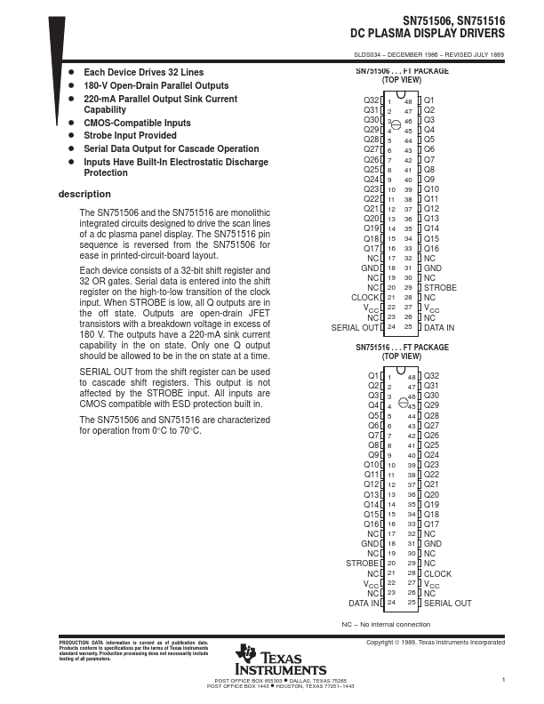
SN751506 . . . FT PACKAGE (TOP VIEW)
Q32 1 48 Q31 2 47 Q30 3 46 Q29 4 45 Q28 5 44 Q27 6 43 Q26 7 42 Q25 8 41 Q24 9 40 Q23 10 39 Q22 11 38 Q21 12 37 Q20 13 36 Q19 14 35 Q18 15 34 Q17 16 33 NC 17 32 GND 18 3...