D Meets ANSI EIA / TIA-232-E and ITU
Recommendation V.28
D Very Low Supply Current D Sleep Mode:
3-State Outputs in High...
D Meets ANSI EIA / TIA-232-E and ITU
Recommendation V.28
D Very Low Supply Current D Sleep Mode:
3-State Outputs in High-Impedance State
Ultra-Low Supply Current . . . 17 µA Typ
D Improved Functional Replacement for:
SN75188,
Motorola MC1488,
National Semiconductor DS14C88, and
DS1488
D
CMOS- and TTL -Compatible Data Inputs D On-Chip Slew-Rate Limit . . . 30 V/µs D Output Current Limit . . . 10 mA Typ D Wide Supply
Voltage Range . . . ± 4.5 V
to ± 15 V
SN75C198 QUADRUPLE LOW-POWER LINE DRIVERS
SLLS051C – JULY 1990 – REVISED MARCH 1997
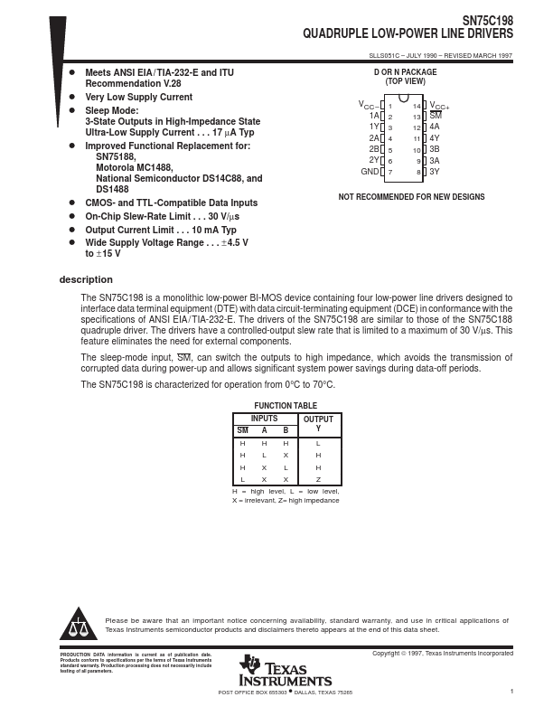
D OR N PACKAGE (TOP VIEW)
VCC – 1 1A 2 1Y 3 2A 4 2B 5 2Y 6
GND 7
14 VCC+ 13 SM 12 4A 11 4Y 10 3B 9 3A 8 3Y
NOT RECOMMENDED FOR NEW DESIGNS
description
The SN75C198 is a monolithic low-power BI-MOS device containing four low-power line drivers designed to interface data terminal equipment (DTE) with data circuit-terminating equipment (DCE) in conformance with the specifications of ANSI EIA / TIA-232-E. The drivers of the SN75C198 are similar to those of the SN75C188 quadruple driver. The drivers have a controlled-output slew rate that is limited to a maximum of 30 V/µs. This feature eliminates the need for external components.
The sleep-mode input, SM, can switch the outputs to high impedance, which avoids the transmission of corrupted data during power-up and allows significant system power savings during data-off periods.
The SN75C198 is characterized for operation from 0°C to 70°C.
FUNCTION TABLE
INPUTS SM A B
OUTPUT Y
HHH
L
HLX
H...