SPV1001N
Cool bypass switch for photovoltaic applications
Features
■ SPV1001N30 IF=12.5 A, VR=30 V ■ SPV1001N40 IF=12.5...
SPV1001N
Cool bypass switch for photovoltaic applications
Features
■ SPV1001N30 IF=12.5 A, VR=30 V ■ SPV1001N40 IF=12.5 A, VR=40 V ■ Very low forward
voltage drop ■ Very low reverse leakage current ■ 150 °C operating junction temperature
Applications
■ Photovoltaic panels
Description
The SPV1001N is a system-in-package solution for photovoltaic applications to perform cool bypass rectification similar to that of a conventional Schottky diode but with much lower forward
voltage drop and reverse leakage current.
The device consists of a power
MOSFET transistor which charges a capacitor during the OFF time, and drives its gate during the ON time using the charge previously stored in the capacitor.
The ON and OFF times are set to reduce the average
voltage drop across the drain and source terminals, resulting in reduced power dissipation.
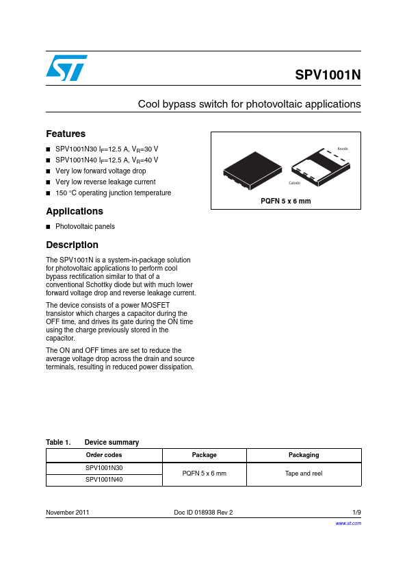
Anodo
Catodo
PQFN 5 x 6 mm
Table 1.
Device summary Order codes SPV1001N30 SPV1001N40
November 2011
Package PQFN 5 x 6 mm
Doc ID 018938 Rev 2
Packaging Tape and reel
1/9
www.st.com
9
Maximum ratings
1 Maximum ratings
SPV1001N
1.1
Absolute maximum ratings
Table 2. Absolute maximum ratings
Symbol
Parameter
Value SPV1001N30 SPV1001N40
VR IF
IFSM
Max DC reverse
voltage
Max forward current
Non repetitive peak surge (half-wave, single phase 50-60 Hz)
ESD level Human body level
30 12.5 250 ≥8 k
40 12.5 250 ≥8 k
Unit
V A A V
1.2
Thermal data
Table 3. Thermal data
Symbol
Parameter
TJ TSTG RthJC
Junction temperature operating ...