Final data
SPW11N60C3
VDS @ Tjmax RDS(on) ID 650 0.38 11
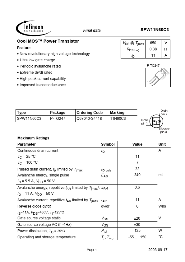
P-TO247
Cool MOS™ Power Transistor
Feature • New revolutionar...
Final data
SPW11N60C3
VDS @ Tjmax RDS(on) ID 650 0.38 11
P-TO247
Cool MOS™ Power Transistor
Feature New revolutionary high
voltage technology Ultra low gate charge Periodic avalanche rated Extreme dv/dt rated High peak current capability Improved transconductance
V Ω A
Type SPW11N60C3
Package P-TO247
Ordering Code Q67040-S4418
Marking 11N60C3
Maximum Ratings Parameter Continuous drain current TC = 25 °C TC = 100 °C Pulsed drain current, tp limited by Tjmax Avalanche energy, single pulse I D = 5.5 A, VDD = 50 V Avalanche energy, repetitive tAR limited by Tjmax1) EAR I D = 11 A, VDD = 50 V Avalanche current, repetitive tAR limited by Tjmax I AR Reverse diode dv/dt dv/dt
IS=11A, VDS=480V, T j=125°C
Symbol ID
Value 11 7
Unit A
I D puls EAS
33 340 0.6 11 6 ±20 ±30 125 -55... +150 W °C 2003-09-17 A V/ns V mJ
Gate source
voltage static Gate source
voltage AC (f >1Hz) Power dissipation, TC = 25°C Operating and storage temperature
Page 1
VGS VGS Ptot T j , T stg
Final data Maximum Ratings Parameter Drain Source
voltage slope
V DS = 480 V, I D = 11 A, Tj = 125 °C
SPW11N60C3
Symbol dv/dt
Value 50
Unit V/ns
Thermal Characteristics Parameter Thermal resistance, junction - case Thermal resistance, junction - ambient, leaded Soldering temperature, 1.6 mm (0.063 in.) from case for 10s Electrical Characteristics, at Tj=25°C unless otherwise specified Parameter Symbol Conditions min. Drain-source breakdown
voltage V(BR)DSS V GS=0V, ID=0.25mA Drain-Source avalan...