Main Product Characteristics:
VDSS
-20V
RDS(on) 49mohm(typ.) ID -7.9A
Features and ...
Main Product Characteristics:
VDSS
-20V
RDS(on) 49mohm(typ.) ID -7.9A
Features and Benefits:
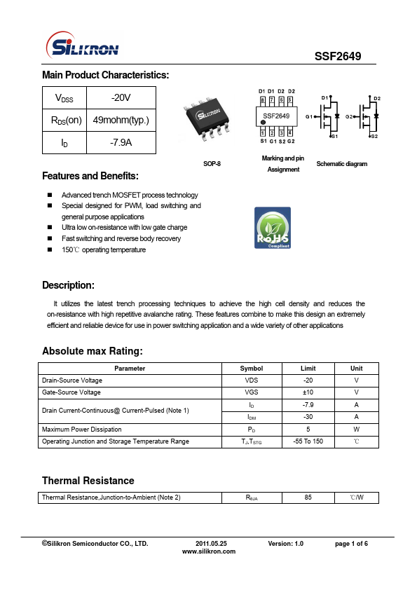
SOP-8
Advanced trench
MOSFET process technology Special designed for PWM, load switching and
general purpose applications Ultra low on-resistance with low gate charge Fast switching and reverse body recovery 150℃ operating temperature
SSF2649
D1 G1
G2
S1
D2 S2
Marking and pin
Assignment
Schematic diagram
Description:
It utilizes the latest trench processing techniques to achieve the high cell density and reduces the on-resistance with high repetitive avalanche rating. These features combine to make this design an extremely efficient and reliable device for use in power switching application and a wide variety of other applications
Absolute max Rating:
Drain-Source
Voltage Gate-Source
Voltage
Parameter
Drain Current-Continuous@ Current-Pulsed (Note 1)
Maximum Power Dissipation Operating Junction and Storage Temperature Range
Symbol VDS VGS ID IDM PD
TJ,TSTG
Limit -20 ±10 -7.9 -30 5 -55 To 150
Unit V V A A W ℃
Thermal Resistance
Thermal Resistance,Junction-to-Ambient (Note 2)
RθJA
85 ℃/W
©Silikron Semiconductor CO., LTD.
2011.05.25 www.silikron.com
Version: 1.0
page 1 of 6
Electrical Characterizes @TA=25℃ unless otherwise specified
Symbol Drain-Source Breakdown
Voltage Zero Gate
Voltage Drain Current Gate-Body Leakage Current Gate Threshold
Voltage
Drain-Source On-St...