SSF3117
www.DataSheet4U.com
DESCRIPTION
The SSF3117 uses advanced trench technology to provide excellent RDS(ON) and lo...
SSF3117
www.DataSheet4U.com
DESCRIPTION
The SSF3117 uses advanced trench technology to provide excellent RDS(ON) and low gate charge . A Schottky diode is provided to facilitate the implementation of a bidirectional blocking switch, or for DC-DC conversion applications.
GENERAL FEATURES
●
MOSFET VDS = -20V,ID = -3.3A RDS(ON) < 180mΩ @ VGS=-1.8V RDS(ON) < 120mΩ @ VGS=-2.5V RDS(ON) < 90mΩ @ VGS=-4.5V ● SCHOTTKY VR = 30V, IF = 2A, VF<0.53V @ 1.0A ● High Power and current handing capability ● Lead free product is acquired ● Surface Mount Package
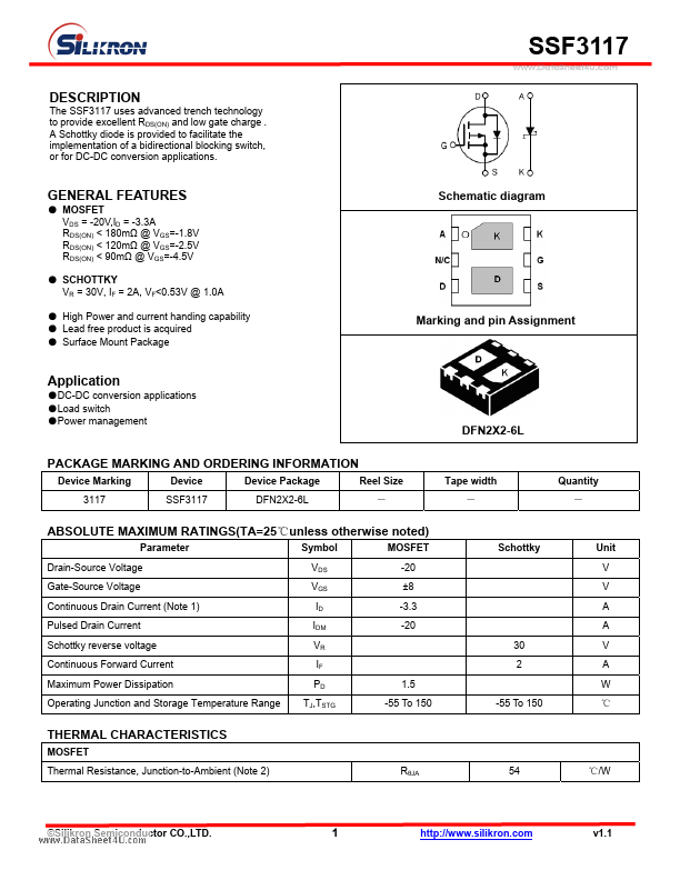
Schematic diagram
Marking and pin Assignment
Application
●DC-DC conversion applications ●Load switch ●Power management
DFN2X2-6L
PACKAGE MARKING AND ORDERING INFORMATION
Device Marking 3117 Device SSF3117 Device Package DFN2X2-6L Reel Size - Tape width - Quantity -
ABSOLUTE MAXIMUM RATINGS(TA=25℃unless otherwise noted)
Parameter Drain-Source
Voltage Gate-Source
Voltage Continuous Drain Current (Note 1) Pulsed Drain Current Schottky reverse
voltage Continuous Forward Current Maximum Power Dissipation Operating Junction and Storage Temperature Range Symbol VDS VGS ID IDM VR IF PD TJ,TSTG 1.5 -55 To 150 -55 To 150
MOSFET -20 ±8 -3.3 -20 30 2 Schottky Unit V V A A V A W ℃
THERMAL CHARACTERISTICS
MOSFET Thermal Resistance, Junction-to-Ambient (Note 2) RθJA 54 ℃/W
©Silikron Semiconductor CO.,LTD.
1
http://www.silikron.com
v1.1
SSF3117
www.DataSheet4U.com
ELECTRICAL CHARACTERISTICS (TA=25℃unless otherwise noted)
Parameter OFF CHAR...