Main Product Characteristics:
VDSS RDS(on)
ID
25 V 6.8 mΩ(typ.)
18A
SOP-8
Features and Benefits:
Advanced MOSFET p...
Main Product Characteristics:
VDSS RDS(on)
ID
25 V 6.8 mΩ(typ.)
18A
SOP-8
Features and Benefits:
Advanced
MOSFET process technology Special designed for PWM, load switching and
general purpose applications Ultra low on-resistance with low gate charge Fast switching and reverse body recovery 150℃ operating temperature
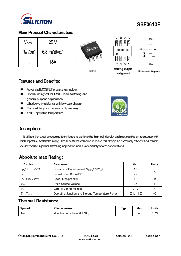
SSF3610E
SSF3610E
Marking and pin Assignment
Schematic diagram
Description:
It utilizes the latest processing techniques to achieve the high cell density and reduces the on-resistance with high repetitive avalanche rating. These features combine to make this design an extremely efficient and reliable device for use in power switching application and a wide variety of other applications.
Absolute max Rating:
Symbol ID @ TC = 25°C IDM PD @TC = 25°C VDS VGS TJ TSTG
Parameter Continuous Drain Current, VGS @ 10V① Pulsed Drain Current② Power Dissipation③ Drain-Source
Voltage Gate-to-Source
Voltage Operating Junction and Storage Temperature Range
Max. 18 72 3.1 25 ± 12
-55 to +150
Thermal Resistance
Symbol RθJA
Characterizes Junction-to-ambient (t ≤ 10s) ④
Typ. —
Max. 40
Units A W V V °C
Units ℃/W
©Silikron Semiconductor CO.,LTD.
2012.05.25 www.silikron.com
Version : 2.1
page 1 of 7
Electrical Characterizes @TA=25℃ unless otherwise specified
Symbol Parameter V(BR)DSS Drain-to-Source breakdown
voltage
RDS(on) Static Drain-to-Source on-resistance
VGS(th) IDSS
IGSS
Qg Qgs Qgd td(on) tr td(off) tf Ciss Coss Crss
Gate threshold
voltage D...