Advanced Power MOSFET
FEATURES
Avalanche Rugged Technology Rugged Gate Oxide Technology
www.DataSheet4U.com
SSW/I1N60A
...
Advanced Power
MOSFET
FEATURES
Avalanche Rugged Technology Rugged Gate Oxide Technology
www.DataSheet4U.com
SSW/I1N60A
BVDSS = 600 V RDS(on) = 12 Ω ID = 1 A
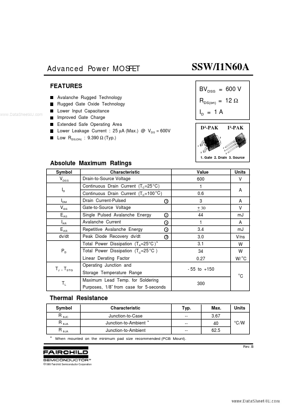
D2-PAK
2
Lower Input Capacitance Improved Gate Charge Extended Safe Operating Area Lower Leakage Current : 25 µA (Max.) @ VDS = 600V Low RDS(ON) : 9.390 Ω (Typ.)
1
I2-PAK
1 3 2 3
1. Gate 2. Drain 3. Source
Absolute Maximum Ratings
Symbol VDSS ID IDM VGS EAS IAR EAR dv/dt PD Characteristic Drain-to-Source
Voltage Continuous Drain Current (TC=25 C ) Continuous Drain Current (TC=100 C ) Drain Current-Pulsed Gate-to-Source
Voltage Single Pulsed Avalanche Energy Avalanche Current Repetitive Avalanche Energy Peak Diode Recovery dv/dt Total Power Dissipation (TA=25 oC ) * Total Power Dissipation (TC=25 C ) Linear Derating Factor TJ , TSTG TL Operating Junction and Storage Temperature Range Maximum Lead Temp. for Soldering Purposes, 1/8” from case for 5-seconds
o o o
Value 600 1 0.6
1 O
Units V A A V mJ A mJ V/ns W W W/ C
o
3 + _ 30 44 1 3.4 3.0 3.1 34 0.27 - 55 to +150
O 1 O 1 O 3 O
2
o
C
300
Thermal Resistance
Symbol R θJC R θ JA R θ JA Characteristic Junction-to-Case Junction-to-Ambient * Junction-to-Ambient Typ. ---Max. 3.67 40 62.5
o
Units C /W
* When mounted on the minimum pad size recommended (PCB Mount).
Rev. B
©1999 Fairchild Semiconductor Corporation
SSW/I1N60A
Symbol BVDSS ∆BV/∆TJ VGS(th)
www.DataSheet4U.com
N-CHANNEL POWER
MOSFET
Electrical Characteristics (TC=25 oC unless otherwise specified)
Char...