SSM6J205FE
TOSHIBA Field-Effect Transistor Silicon P-Channel MOS Type
SSM6J205FE
High-Speed Switching Applications Powe...
SSM6J205FE
TOSHIBA Field-Effect Transistor Silicon P-Channel MOS Type
SSM6J205FE
High-Speed Switching Applications Power Management Switch Applications
1.8V drive P-ch 2-in-1 Low ON-resistance: Unit: mm
Ron = 460 mΩ (max) (@VGS = −1.8 V) Ron = 306 mΩ (max) (@VGS = −2.5 V) Ron = 234 mΩ (max) (@VGS = −4.0 V)
www.DataSheet4U.com
Absolute Maximum Ratings (Ta = 25°C)
Characteristic Drain-source
voltage Gate-source
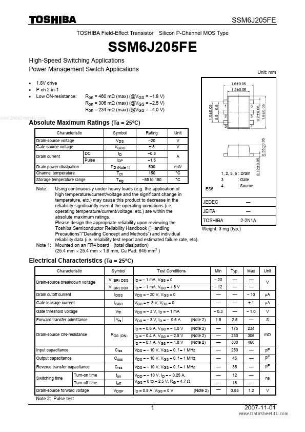
voltage Drain current Drain power dissipation Channel temperature Storage temperature range DC Pulse Symbol VDS VGSS ID IDP PD (Note 1) Tch Tstg Rating −20 ±8 −0.8 −1.6 500 150 −55 to 150 Unit V V A mW °C °C ES6 1, 2, 5, 6 : Drain 3 4 : Gate : Source
Note:
Using continuously under heavy loads (e.g. the application of high temperature/current/
voltage and the significant change in temperature, etc.) may cause this product to decrease in the reliability significantly even if the operating conditions (i.e. operating temperature/current/
voltage, etc.) are within the absolute maximum ratings. Please design the appropriate reliability upon reviewing the Toshiba Semiconductor Reliability Handbook (“Handling Precautions”/“Derating Concept and Methods”) and individual reliability data (i.e. reliability test report and estimated failure rate, etc). Note 1: Mounted on an FR4 board (total dissipation) 2 (25.4 mm × 25.4 mm × 1.6 mm, Cu Pad: 645 mm )
JEDEC JEITA TOSHIBA
― ― 2-2N1A
Weight: 3 mg (typ.)
Electrical Characteristics (Ta = 25°C)
Characteristic Drain-source bre...