SSM6L13TU www.DataSheet4U.com
TOSHIBA Field-Effect Transistor Silicon P / N Channel MOS Type
SSM6L13TU
Power Management...
SSM6L13TU www.DataSheet4U.com
TOSHIBA Field-Effect Transistor Silicon P / N Channel MOS Type
SSM6L13TU
Power Management Switch Applications High-Speed Switching Applications
1.8 V drive P–ch , N–ch 2–in–1 Low ON–resistance: Pch : Nch
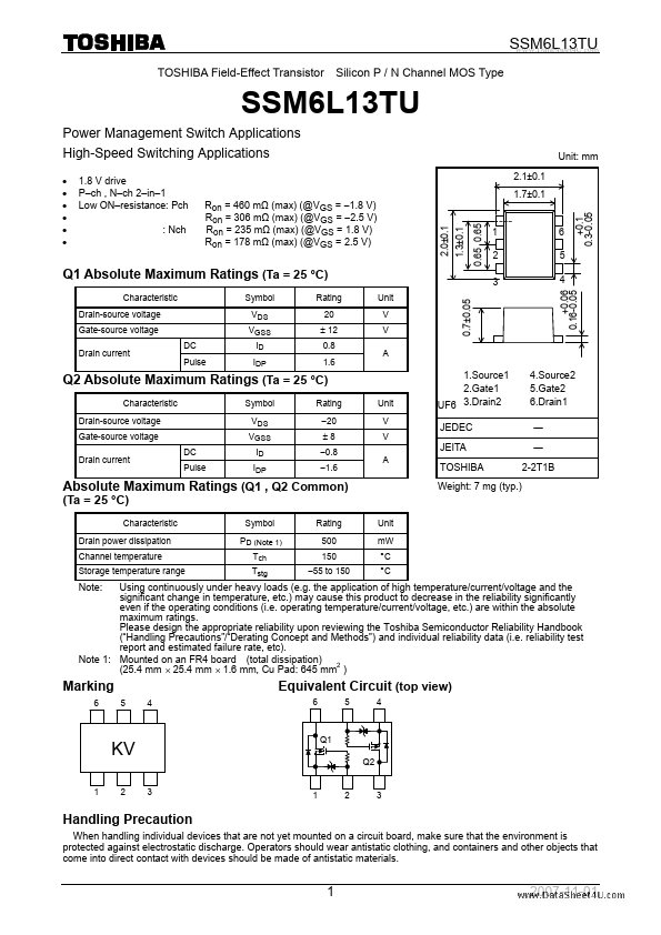
2.1±0.1 1.7±0.1 0.65 0.65 +0.1 0.3-0.05
Unit: mm
2.0±0.1
1.3±0.1
Ron = 460 mΩ (max) (@VGS = −1.8 V) Ron = 306 mΩ (max) (@VGS = −2.5 V) Ron = 235 mΩ (max) (@VGS = 1.8 V) Ron = 178 mΩ (max) (@VGS = 2.5 V)
1 2 3
6 5 4
Q1 Absolute Maximum Ratings (Ta = 25 °C)
Drain-source
voltage Gate-source
voltage Drain current DC Pulse VDS VGSS ID IDP 20 ± 12 0.8 1.6 V V A
0.7±0.05
Characteristic
Symbol
Rating
Unit
Q2 Absolute Maximum Ratings (Ta = 25 °C)
Characteristic Drain-source
voltage Gate-source
voltage Drain current DC Pulse Symbol VDS VGSS ID IDP Rating −20 ±8 −0.8 −1.6 Unit V V A
1.Source1 2.Gate1 UF6 3.Drain2 JEDEC JEITA TOSHIBA Weight: 7 mg (typ.)
4.Source2 5.Gate2 6.Drain1 ― ― 2-2T1B
(Ta = 25 °C)
Absolute Maximum Ratings (Q1 , Q2 Common)
Characteristic Drain power dissipation Channel temperature Storage temperature range Symbol PD (Note 1) Tch Tstg Rating 500 150 −55 to 150 Unit mW °C °C
Note:
Using continuously under heavy loads (e.g. the application of high temperature/current/
voltage and the significant change in temperature, etc.) may cause this product to decrease in the reliability significantly even if the operating conditions (i.e. operating temperature/current/
voltage, etc.) are within the absolute maximum rati...