SSM6N05FU
TOSHIBA Field Effect Transistor Silicon N Channel MOS Type
SSM6N05FU
High Speed Switching Applications
Unit:...
SSM6N05FU
TOSHIBA Field Effect Transistor Silicon N Channel MOS Type
SSM6N05FU
High Speed Switching Applications
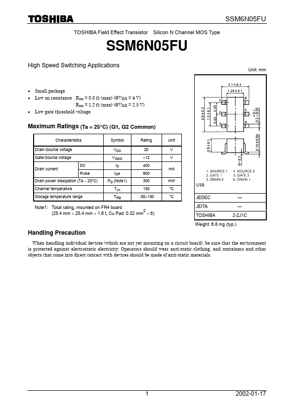
Unit: mm
· Small package · Low on resistance : Ron = 0.8 Ω (max) (@VGS = 4 V)
: Ron = 1.2 Ω (max) (@VGS = 2.5 V) · Low gate threshold
voltage
Maximum Ratings (Ta = 25°C) (Q1, Q2 Common)
Characteristics
Symbol
Rating
Unit
Drain-Source
voltage
VDS
20
V
Gate-Source
voltage
VGSS
±12
V
Drain current
DC Pulse
ID
400 mA
IDP
800
Drain power dissipation (Ta = 25°C)
PD (Note1)
300
mW
Channel temperature
Tch
150
°C
Storage temperature range
Tstg
-55~150
°C
JEDEC
―
Note1: Total rating, mounted on FR4 board (25.4 mm ´ 25.4 mm ´ 1.6 t, Cu Pad: 0.32 mm2 ´ 6)
JEITA TOSHIBA
― 2-2J1C
Weight: 6.8 mg (typ.)
Handling Precaution
When handling individual devices (which are not yet mounting on a circuit board), be sure that the environment is protected against electrostatic electricity. Operators should wear anti-static clothing, and containers and other objects that come into direct contact with devices should be made of anti-static materials.
1
2002-01-17
Marking
6
5
4
DF
1
2
3
Equivalent Circuit (top view)
6
5
4
Q1 Q2
1
2
3
SSM6N05FU
Electrical Characteristics (Ta = 25°C) (Q1, Q2 common)
Characteristics
Gate leakage current Drain-Source breakdown
voltage Drain cut-off current Gate threshold
voltage Forward transfer admittance
Drain-Source ON resistance
Input capacitance
Reverse transfer capacitance
Output capacitance
S...