SSM6N43FU
TOSHIBA Field-Effect Transistor Silicon N Channel MOS Type
SSM6N43FU
○ High-Speed Switching Applications
• • ...
SSM6N43FU
TOSHIBA Field-Effect Transistor Silicon N Channel MOS Type
SSM6N43FU
○ High-Speed Switching Applications
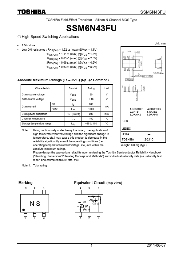
1.5-V drive Low ON-resistance : RDS(ON) = 1.52 Ω (max) (@VGS = 1.5V) : RDS(ON) = 1.14 Ω (max) (@VGS = 1.8V) : RDS(ON) = 0.85 Ω (max) (@VGS = 2.5V) : RDS(ON) = 0.66 Ω (max) (@VGS = 4.5V) : RDS(ON) = 0.63 Ω (max) (@VGS = 5.0V) Unit: mm
Absolute Maximum Ratings (Ta = 25°C) (Q1,Q2 Common)
Characteristic Drain-source
voltage Gate-source
voltage Drain current Drain power dissipation Channel temperature Storage temperature range DC Pulse Symbol VDSS VGSS ID IDP PD (Note1) Tch Tstg Rating 20 ± 10 500 1000 200 150 −55 to 150 Unit V V mA mW °C °C
1.SOURCE1 2.GATE1 3.DRAIN2
4.SOURCE2 5.GATE2 6.DRAIN1
US6
Note:
JEDEC ― Using continuously under heavy loads (e.g. the application of high temperature/current/
voltage and the significant change in JEITA ― temperature, etc.) may cause this product to decrease in the TOSHIBA 2-2J1C reliability significantly even if the operating conditions (i.e. operating temperature/current/
voltage, etc.) are within the Weight: 6.8 mg (typ.) absolute maximum ratings. Please design the appropriate reliability upon reviewing the Toshiba Semiconductor Reliability Handbook (“Handling Precautions”/“Derating Concept and Methods”) and individual reliability data (i.e. reliability test report and estimated failure rate, etc).
Note 1: Total rating
Marking
6 5 4
Equivalent Circuit (top view)
6 5 4
NS
1 2 3 1
Q1
Q2
2
3
1
2011-06-07
SSM6N...