MOSFETs Silicon N-Channel MOS
SSM6N67NU
1. Applications
• Power Management Switches • DC-DC Converters
2. Features
(1) A...
MOSFETs Silicon N-Channel MOS
SSM6N67NU
1. Applications
Power Management Switches DC-DC Converters
2. Features
(1) AEC-Q101 qualified (Note 1) (2) 1.8-V gate drive
voltage. (3) Low drain-source on-resistance
: RDS(ON) = 39.1 mΩ (max) (@VGS = 4.5 V) RDS(ON) = 53 mΩ (max) (@VGS = 2.5 V) RDS(ON) = 82 mΩ (max) (@VGS = 1.8 V)
Note 1: For detail information, please contact to our sales.
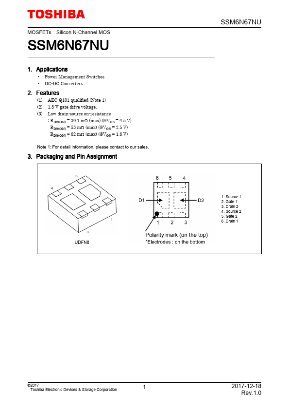
3. Packaging and Pin Assignment
UDFN6
SSM6N67NU
1. Source 1 2. Gate 1 3. Drain 2 4. Source 2 5. Gate 2 6. Drain 1
©2017 Toshiba Electronic Devices & Storage Corporation
1
2017-12-18 Rev.1.0
SSM6N67NU
4. Absolute Maximum Ratings (Note) (Unless otherwise specified, Ta = 25 ) (Q1,Q2 Common)
Characteristics
Symbol
Rating
Unit
Drain-source
voltage
VDSS 30 V
Gate-source
voltage
VGSS
12/-8
Drain current (DC)
(Note 1)
ID
4A
Drain current (pulsed)
(Note 1), (Note 2)
IDP
10
Power dissipation
(Note 3)
PD
1W
Power dissipation
(t ≤ 10 s)
(Note 3)
PD
2W
Channel temperature
Tch 150
Storage temperature
Tstg -55 to 150
Note: Using continuously under heavy loads (e.g. the application of high temperature/current/
voltage and the significant change in temperature, etc.) may cause this product to decrease in the reliability significantly even if the operating conditions (i.e. operating temperature/current/
voltage, etc.) are within the absolute maximum ratings. Please design the appropriate reliability upon reviewing the Toshiba Semiconductor Reliability Handbook ("Handling Preca...