SSM6P47NU
TOSHIBA Field Effect Transistor Silicon P Channel MOS Type(U-MOS VI)
SSM6P47NU
Power Management Switch Applic...
SSM6P47NU
TOSHIBA Field Effect Transistor Silicon P Channel MOS Type(U-MOS VI)
SSM6P47NU
Power Management Switch Applications
1.5V drive Low ON-resistance: RDS(on) = 242 mΩ (max) (@VGS = -1.5 V) RDS(on) = 170 mΩ (max) (@VGS = -1.8 V) RDS(on) = 125 mΩ (max) (@VGS = -2.5 V) RDS(on) = 95 mΩ (max) (@VGS = -4.5 V)
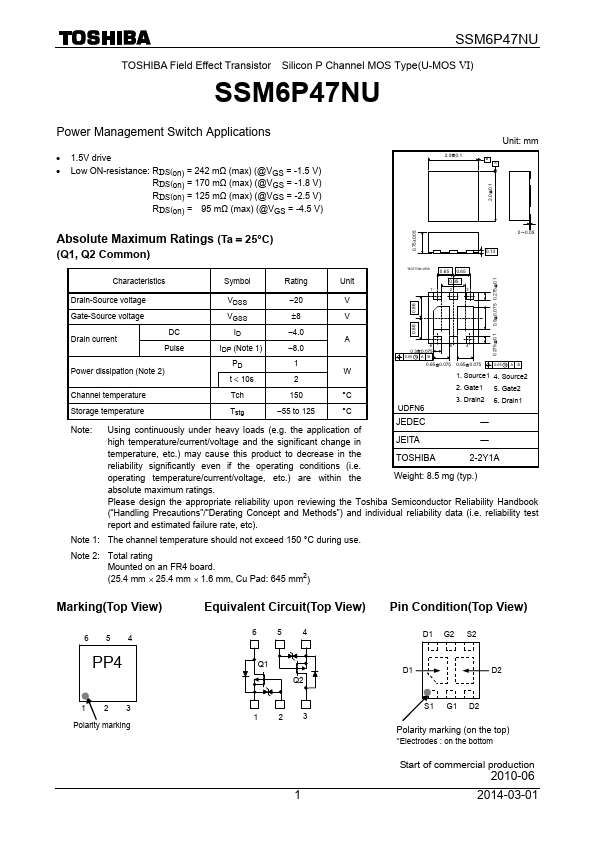
0.75±0.05 2.0±0.1
B A
Unit: mm
2.0±0.1
Absolute Maximum Ratings (Ta = 25°C)
(Q1, Q2 Common)
Characteristics Drain-Source
voltage Gate-Source
voltage Drain current DC Pulse Symbol VDSS VGSS ID IDP (Note 1) PD t < 10s Tch Tstg Rating −20 ±8 −4.0 −8.0 1 2 150 −55 to 125 Unit
0~0.05
0.13
*BOTTOM VIEW
0.65
0.65 0.95 0.9±0.075 0.275±0.1 0.275±0.1
0.05 M A
1
2
3
V A
0.86
0.86
V
6
5
4
0.3±0.075
0.05 M A B
Power dissipation (Note 2) Channel temperature Storage temperature
W °C °C UDFN6
0.65±0.075
0.65±0.075
B
1. Source1 4. Source2 2. Gate1 3. Drain2 5. Gate2 6. Drain1
Note:
JEDEC ― Using continuously under heavy loads (e.g. the application of JEITA ― high temperature/current/
voltage and the significant change in temperature, etc.) may cause this product to decrease in the TOSHIBA 2-2Y1A reliability significantly even if the operating conditions (i.e. Weight: 8.5 mg (typ.) operating temperature/current/
voltage, etc.) are within the absolute maximum ratings. Please design the appropriate reliability upon reviewing the Toshiba Semiconductor Reliability Handbook (“Handling Precautions”/“Derating Concept and Methods”) and individual reliability data (i....