SSS2323
P-Channel Enhancement Mode MOSFET
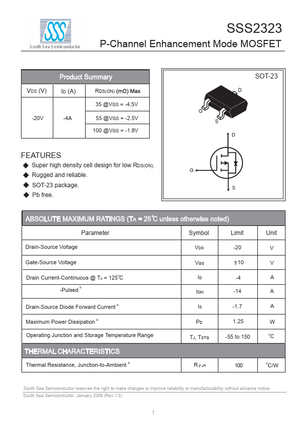
Product Summary
VDS (V) ID (A)
RDS(ON) 35 @VGS = -4.5V -20V -4A 55 @VGS = -2.5...
SSS2323
P-Channel Enhancement Mode
MOSFET
Product Summary
VDS (V) ID (A)
RDS(ON) 35 @VGS = -4.5V -20V -4A 55 @VGS = -2.5V 100 @VGS = -1.8V
G S D
SOT-23
D
FEATURES
Super high density cell design for low RDS(ON). Rugged and reliable. SOT-23 package. Pb free.
o
G S
ABSOLUTE MAXIMUM RATINGS (TA = 25 C unless otherwise noted)
Parameter
Drain-Source
Voltage Gate-Source
Voltage Drain Current-Continuous @ TJ = 125 C -Pulsed
b o
Symbol
VDS VGS ID IDM
a
Limit
-20 + - 10 -4 -14 -1.7 1.25 -55 to 150
Unit
V V A A A W
o
Drain-Source Diode Forward Current Maximum Power Dissipation
a
IS PD TJ, TSTG
Operating Junction and Storage Temperature Range
C
THERMAL CHARACTERISTICS
Thermal Resistance, Junction-to-Ambient
a
R
JA
100
o
C/W
South Sea Semiconductor reserves the right to make changes to improve reliability or manufacturability without advance notice. South Sea Semiconductor, January 2008 (Rev 1.0)
1
SSS2323
P-Channel Electrical Characteristics (TA = 25 C unless otherwise noted)
Parameter
Drain-Source Breakdown
Voltage Zero Gate
Voltage Drain Current Gate-Body Leakage Gate Threshold
Voltage
o
Symbol
BVDSS IDSS IGSS VGS(th)
Condition
VGS=0V, ID=-250 A
Min
-20
Typ
c
Max
Unit
V
VDS=-16V, VGS=0V VGS= 8V, VDS =0V A -0.4 29 48 88 -10 13 1100 240 170 25 45 80 60 13 2 3.8 0.8
-1 100 -1.0 35 55 100 m
A nA V
VDS=VGS ID=-250
VGS=-4.5V, ID=-5.0A Drain-Source On-State Resistance RDS(ON) VGS=-2.5V, ID=-3.0A VGS=-1.8V, ID=-1.5A On-State Drain Current Forward Transconductan...