|
|
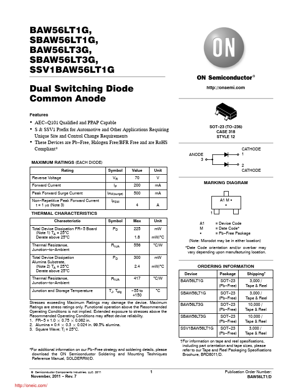
Dual Switching Diode Common Anode
BAW56LT1G, SBAW56LT1G, BAW56LT3G, SBAW56LT3G, SSV1BAW56LT1G Dual Switching Diode Common Anode Features AEC−Q101 Qual...
| @ 2014 :: Datasheetspdf.com :: Semiconductors datasheet search & download site. (Privacy Policy & Contact) |