SSW7N60B / SSI7N60B
November 2001
SSW7N60B / SSI7N60B
600V N-Channel MOSFET
General Description
These N-Channel enhanc...
SSW7N60B / SSI7N60B
November 2001
SSW7N60B / SSI7N60B
600V N-Channel
MOSFET
General Description
These N-Channel enhancement mode power field effect transistors are produced using Fairchild’s proprietary, planar, DMOS technology. This advanced technology has been especially tailored to minimize on-state resistance, provide superior switching performance, and withstand high energy pulse in the avalanche and commutation mode. These devices are well suited for high efficiency switch mode power supplies.
Features
7.0A, 600V, RDS(on) = 1.2Ω @VGS = 10 V Low gate charge ( typical 38 nC) Low Crss ( typical 23 pF) Fast switching 100% avalanche tested Improved dv/dt capability
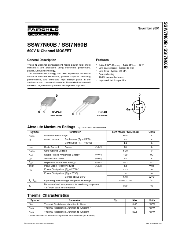
D
D
!
!
#
"
! !
G
S
D2-PAK
SSW Series
G D S
I2-PAK
SSI Series
G!
!
S
Absolute Maximum Ratings
Symbol VDSS ID IDM VGSS EAS IAR EAR dv/dt PD
TC = 25°C unless otherwise noted
Parameter Drain-Source
Voltage - Continuous (TC = 25°C) Drain Current - Continuous (TC = 100°C) Drain Current - Pulsed
(Note 1)
SSW7N60B / SSI7N60B 600 7.0 4.4 28 ± 30
(Note 2) (Note 1) (Note 1) (Note 3)
Units V A A A V mJ A mJ V/ns W W W/°C °C °C
Gate-Source
Voltage Single Pulsed Avalanche Energy Avalanche Current Repetitive Avalanche Energy Peak Diode Recovery dv/dt Power Dissipation (TA = 25°C) *
420 7.0 14.7 5.5 3.13 147 1.18 -55 to +150 300
TJ, Tstg TL
Power Dissipation (TC = 25°C) - Derate above 25°C Operating and Storage Temperature Range Maximum lead temperature for soldering purposes, 1/8! from case f...