ST25N10
N Channel Enhancement Mode MOSFET
25.0A
DESCRIPTION
ST25N10 is the N-Channel logic enhancement mode power field ...
ST25N10
N Channel Enhancement Mode
MOSFET
25.0A
DESCRIPTION
ST25N10 is the N-Channel logic enhancement mode power field effect transistor which is produced using high cell density, DMOS trench technology. The ST16N10 has been designed specially to improve the overall efficiency of DC/DC converters using either synchronous or conventional switching PWM controllers. It has been optimized for low gate charge, low RDS(ON) and fast switching speed.
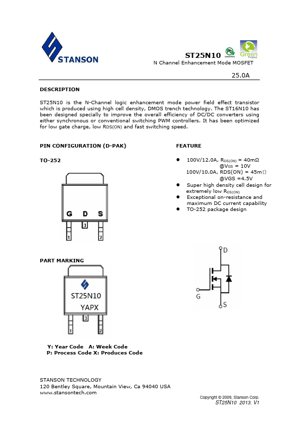
PIN CONFIGURATION (D-PAK) TO-252
FEATURE
100V/12.0A, RDS(ON) = 40mΩ @VGS = 10V
100V/10.0A, RDS(ON) = 45mΩ @VGS =4.5V
Super high density cell design for extremely low RDS(ON) Exceptional on-resistance and maximum DC current capability TO-252 package design
PART MARKING
Y: Year Code A: Week Code P: Process Code X: Produces Code
STANSON TECHNOLOGY 120 Bentley Square, Mountain View, Ca 94040 USA www.stansontech.com
Copyright © 2009, Stanson Corp.
ST25N10 2013. V1
ST25N10
N Channel Enhancement Mode
MOSFET
25.0A
SOULTE MAXIMUM RATINGS (Ta = 25℃ Unless otherwise noted )
Parameter
Symbol Typical
Drain-Source
Voltage
VDSS
100
Gate-Source
Voltage
Continuous Drain Current (TJ=150℃)
Pulsed Drain Current
TA=25℃ TA=100℃
VGSS ID
IDM
±20
25.0 16.0
75
Continuous Source Current (Diode Conduction)
IS
25
Power Dissipation
TA=25℃
PD
79
Operation Junction Temperature
TJ 150
Storgae Temperature Range
TSTG
-55/150
Thermal Resistance-Junction to Ambient
RθJA
110
Unit V V A A A W ℃ ℃
℃/W
STANSON TECHNOLOGY 120 Bentley Square, Mou...