STB16N90K5
Datasheet
N-channel 900 V, 280 mΩ typ., 15 A MDmesh K5 Power MOSFET in a D²PAK package
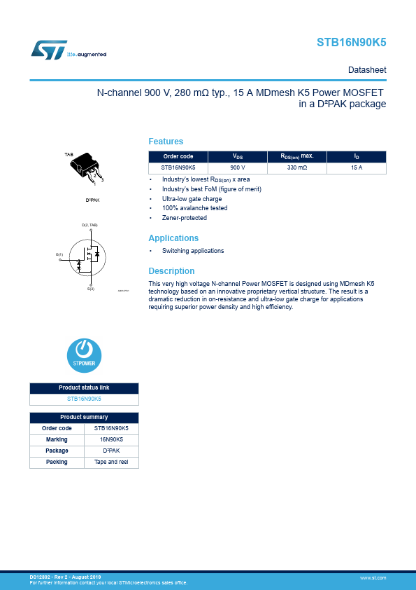
TAB 2 3 1
D²PAK
D(2, ...
STB16N90K5
Datasheet
N-channel 900 V, 280 mΩ typ., 15 A MDmesh K5 Power
MOSFET in a D²PAK package
TAB 2 3 1
D²PAK
D(2, TAB)
G(1)
S(3)
AM01475V1
Features
Order code
VDS
STB16N90K5
900 V
Industry’s lowest RDS(on) x area Industry’s best FoM (figure of merit) Ultra-low gate charge 100% avalanche tested Zener-protected
RDS(on) max. 330 mΩ
ID 15 A
Applications
Switching applications
Description
This very high
voltage N-channel Power
MOSFET is designed using MDmesh K5 technology based on an innovative proprietary vertical structure. The result is a dramatic reduction in on-resistance and ultra-low gate charge for applications requiring superior power density and high efficiency.
Product status link STB16N90K5
Product summary
Order code
STB16N90K5
Marking
16N90K5
Package
D²PAK
Packing
Tape and reel
DS12802 - Rev 2 - August 2019 For further information contact your local STMicroelectronics sales office.
www.st.com
STB16N90K5
Electrical ratings
1 Electrical ratings
Table 1. Absolute maximum ratings
Symbol
Parameter
VGS Gate-source
voltage
ID Drain current (continuous) at TC = 25 °C
ID Drain current (continuous) at TC = 100 °C
ID (1)
Drain current (pulsed)
PTOT
Total power dissipation at TC = 25 °C
dv/dt (2) Peak diode recovery
voltage slope
dv/dt (3)
MOSFET dv/dt ruggedness
Tj Operating junction temperature range
Tstg Storage temperature range
1. Pulse width limited by safe operating area. 2. ISD ≤ 15 A, di/dt ≤ 100 A/μs; VDS peak ≤...