S T U/D420S
S amHop Microelectronics C orp.
J uly 05 , 2006
N-C hannel Logic Level E nhancement Mode Field E ffect Tra...
S T U/D420S
S amHop Microelectronics C orp.
J uly 05 , 2006
N-C hannel Logic Level E nhancement Mode Field E ffect Transistor
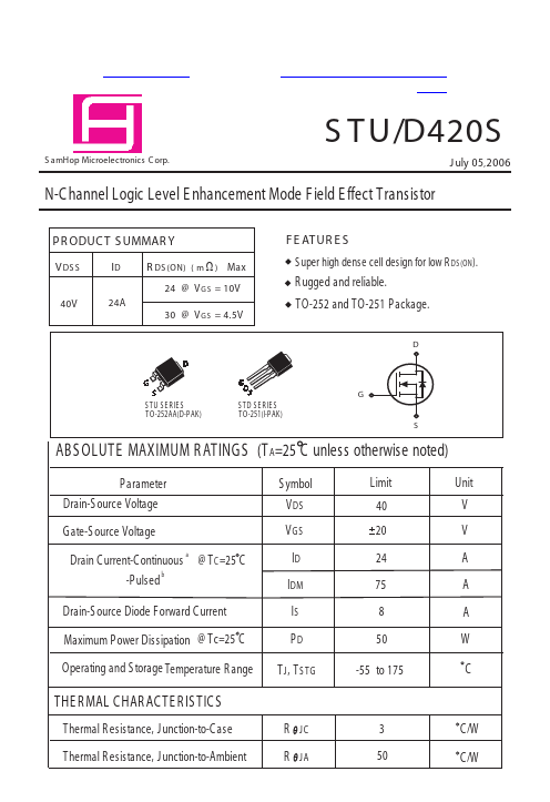
P R ODUC T S UMMAR Y
V DS S
40V
F E AT UR E S
( mW)
ID
24A
R DS (ON)
Max
S uper high dense cell design for low R DS (ON ).
24 @ V G S = 10V 30 @ V G S = 4.5V
R ugged and reliable. TO-252 and TO-251 P ackage.
D
D G S
G D
S
G
S TU S E R IE S TO-252AA(D-P AK)
S TD S E R IE S TO-251(l-P AK)
S
ABS OLUTE MAXIMUM R ATINGS (T A=25 C unless otherwise noted)
P arameter Drain-S ource
Voltage Gate-S ource
Voltage Drain C urrent-C ontinuous b -P ulsed
a
S ymbol V DS V GS @ T C =25 C ID IDM IS PD T J , T S TG
Limit 40 20 24 75 8 50 -55 to 175
Unit V V A A A W C
Drain-S ource Diode Forward C urrent Maximum P ower Dissipation @ Tc=25 C Operating and S torage Temperature R ange
THE R MAL C HAR AC TE R IS TIC S
Thermal R esistance, Junction-to-C ase Thermal R esistance, Junction-to-Ambient R JC R JA 3 50 C /W C /W
S T U/D420S
E LE CTR ICAL CHAR ACTE R IS TICS (T C =25 C unless otherwise noted)
Parameter
5
S ymbol
BV DS S IDS S IGS S
a
Condition
V GS = 0V, ID = 250uA V DS = 32V, V GS = 0V V GS = 20V, V DS = 0V V DS = V GS , ID = 250uA V GS =10V, ID = 10A V GS =4.5V, ID= 8A V DS = 10V, V GS = 10V V DS = 10V, ID = 10A
Min Typ C Max Unit
40 1 10 1 1.9 17 23.5 30 16 750 110 65 3 13 10 37 12 15 7 2.5 4 3 24 V uA uA V
OFF CHAR ACTE R IS TICS
Drain-S ource Breakdown
Voltage Zero Gate
Voltage Drain Current Gate-Body Leakage
ON CHAR ACTE R IS TICS
Gate T...